Beginner's guide to designing a circuit with kicad 6.0
A complete beginner's guide to making a circuit with Kicad 6.0

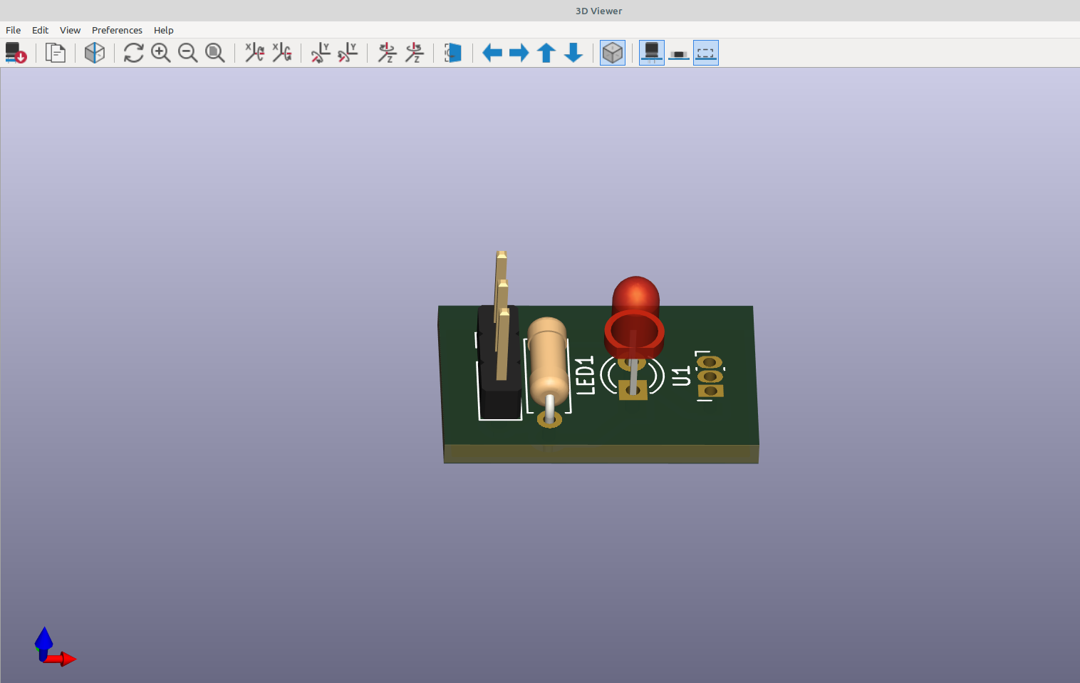
If you have never used kicad to design a circuit here is an introduction to the basics to get you familiar with the program. I am using the hall sensor circuit that I used for the end stop switches when I built the pvc 3d printer because it is a very simple circuit and I have had zero problems with it since I made it, hundreds of prints over 5 years and they still work the same as the day I first turned them on.
I'm going to assume that if you are reading this you know how to download and install the software so I will skip all of that, here is a link to download the software:
The following steps are for a complete beginner, as with anything the more you become familiar with the software the better you will get at it, there are a lot of features and it can be hard to find some of them, but if you are interested in electronics as a hobby it's well worth the effort.
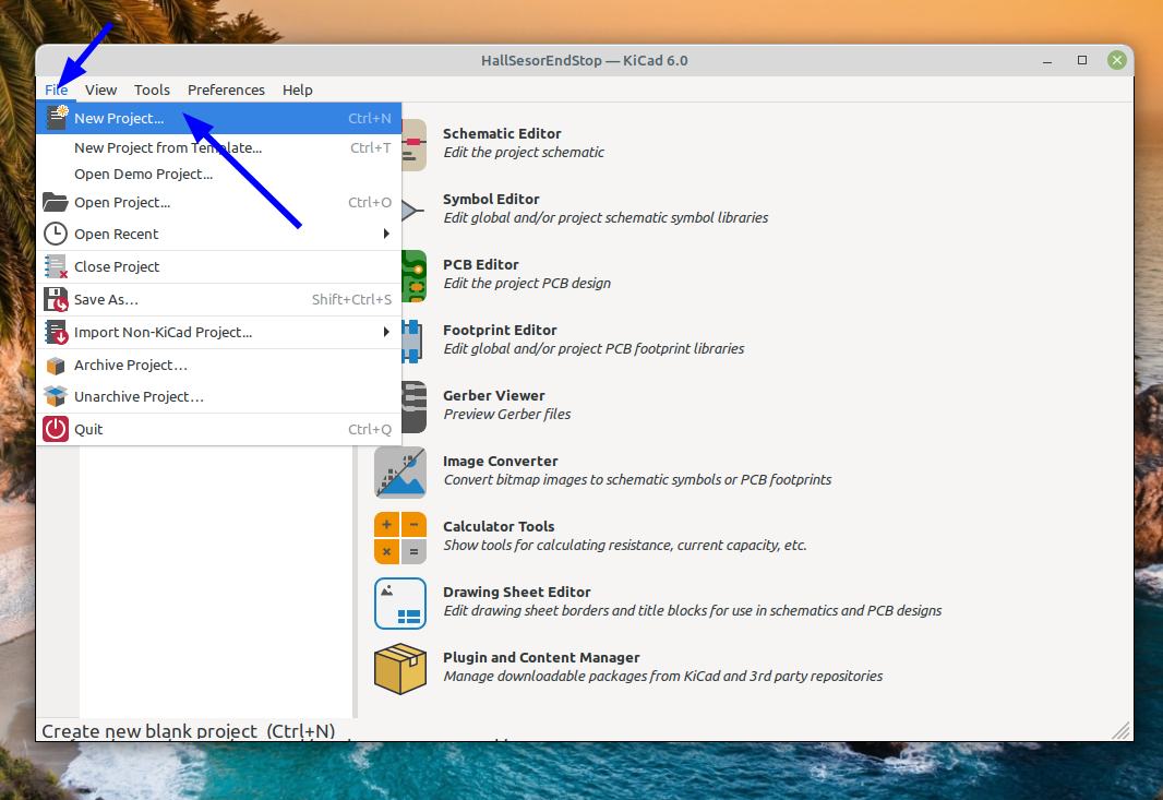
After installation you will open the program and create a new project:
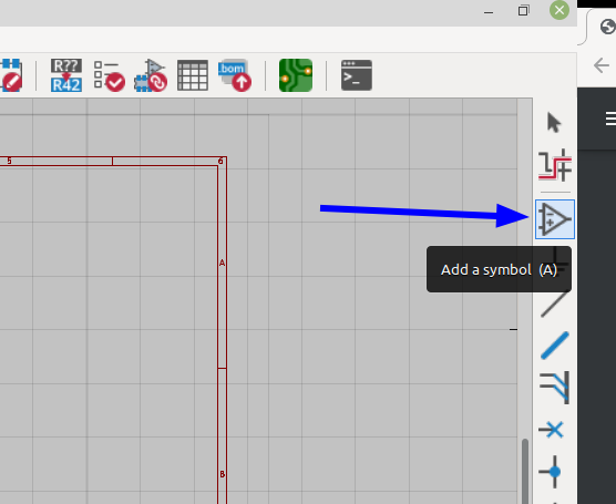
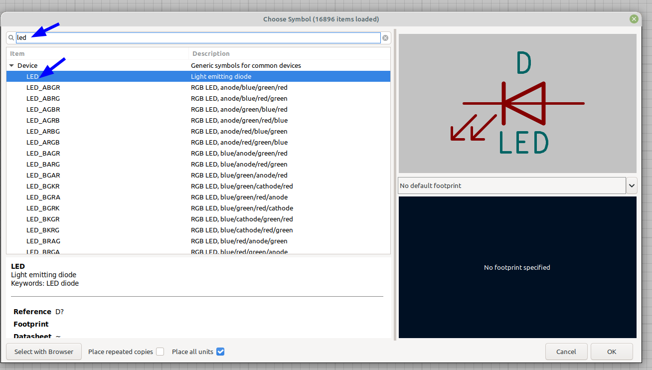
After selecting a location folder and giving it a name double click on the schematic editor icon to start a new schematic, on the right hand side there is an icon to add a new symbol, click on it to add a new component symbol:
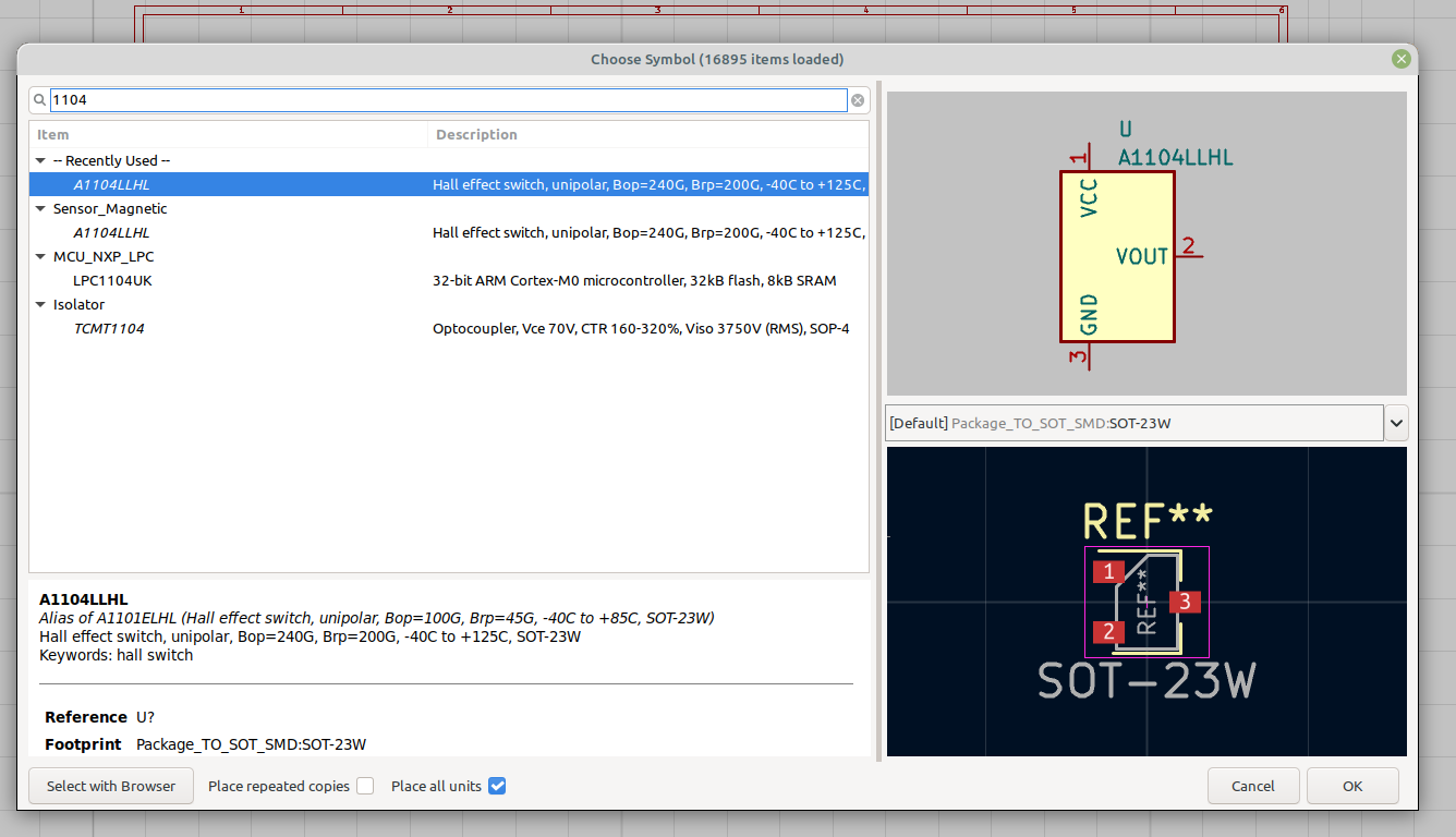
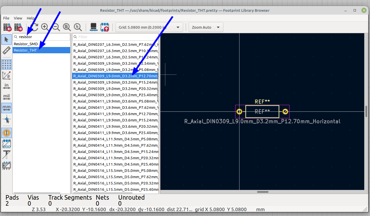
It helps to have all of the parts you are going to use before you start so you know what size they all are, how you are going to mount them on the board and what size holes you need to drill if they are through hole components.If you don't have the components or are unsure what the pin spacing needs to be a data sheet for pretty much every component ever made is available. I am using an A1104 hall sensor so I downloaded the data sheet to see what the package type was, power input required and sensing range:
https://www.allegromicro.com/-/media/files/datasheets/a110x-datasheet.ashx

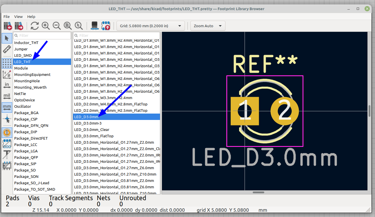
Now that I know what package I need to mount the device I can select it from a list in kicad and assign the correct "foot print" to it :
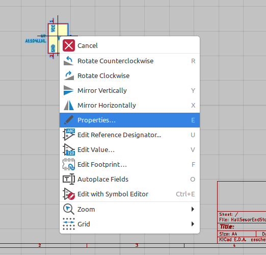
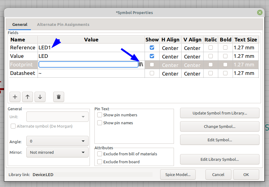
In the picture above I have the correct device but the foot print is for a surface mount device and I need a through hole foot print, so I will change it. After clicking ok the component will show up and you can click on the schematic to drop it in place, right click on the component and select properties, a new window will pop up allowing the various parameters of the component to be changed:
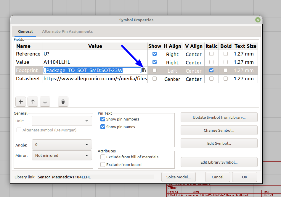
Here we can change the name, value etc. To change the footprint click on the icon that looks like three books as shown above.
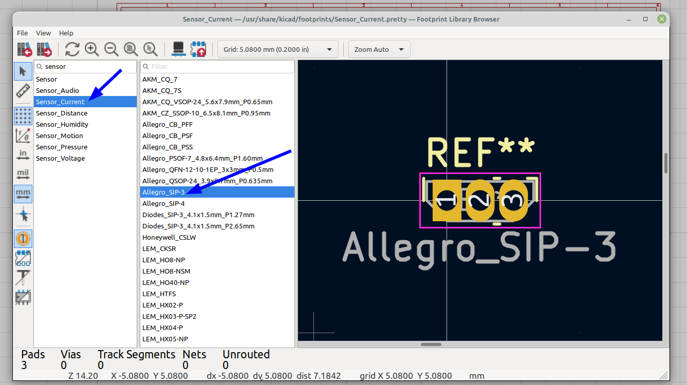
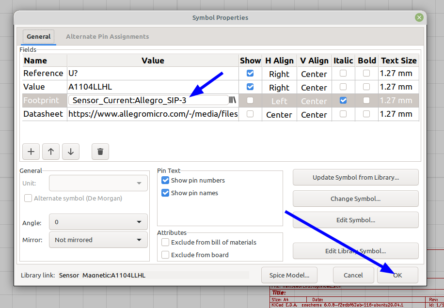
You can type in a description in the search box and a list of different components and foot prints will show up, usually you can find the exact component or one with a similar foot print that will work, once you have it selected double click on the one you have highlighted and it will assign that footprint to your component.
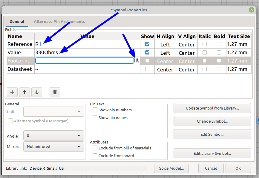
After clicking ok we can add more components, assign a name, value and foot print to them in the exact same way, here is the led:
and the resistor:
Once we have all of our components on the schematic we can add wires to connect them:
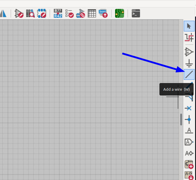
Once you click on add a wire there will be a pen next to the mouse cursor, click on a pin of the device you are wanting to add a wire to and drag the mouse it will show the wire. Then route the wire to the pin of another device and click again and it will connect the wire to the new device, once the wire is routed you can select it an move it to different positions to place it where you need to.
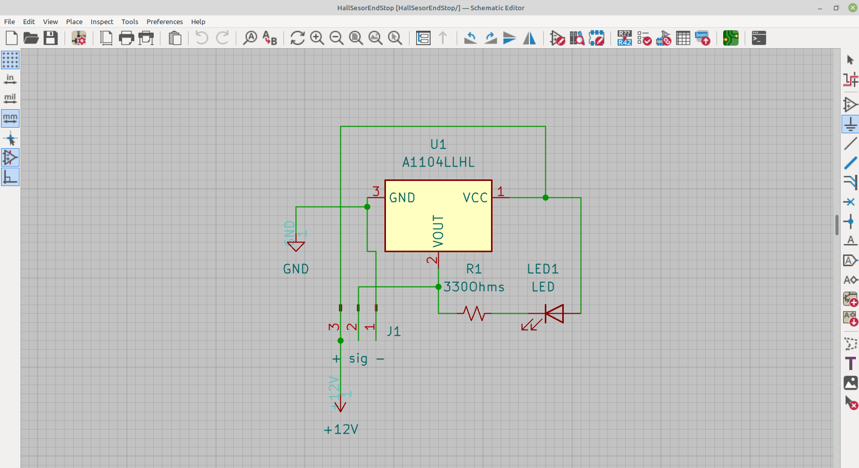
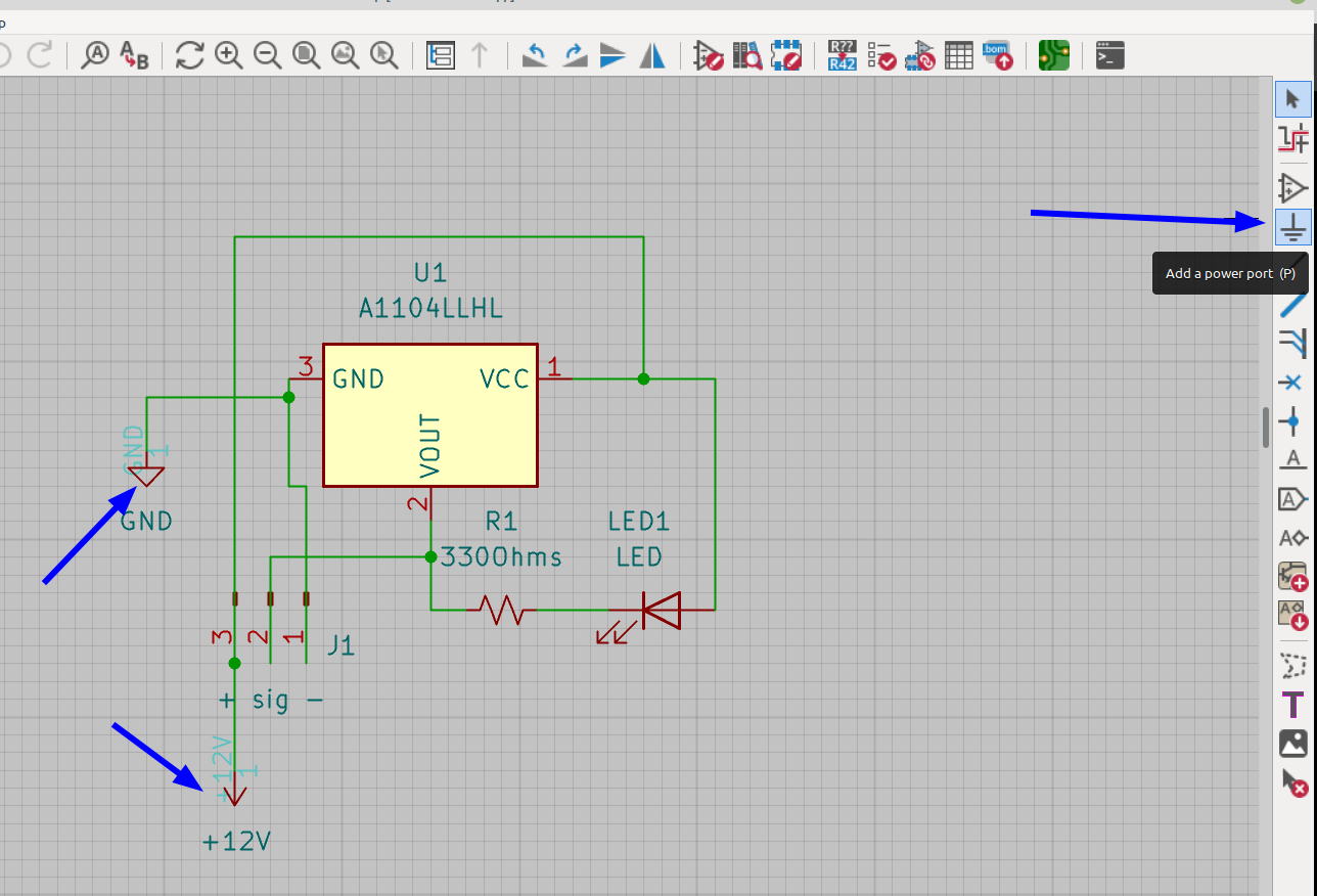
You'll notice that where the wires connect together there is a circle indicating a junction, you can also change the color of the wires by right clicking on them and selecting properties and changing their width, style or color it's pretty self explanatory.
I also added a +12v and GND connection power port, this is handy for later on when you make the the pcb, any point that needs to be connected to ground can connect to the ground plane copper pour which greatly reduces the number of traces needed on the board.
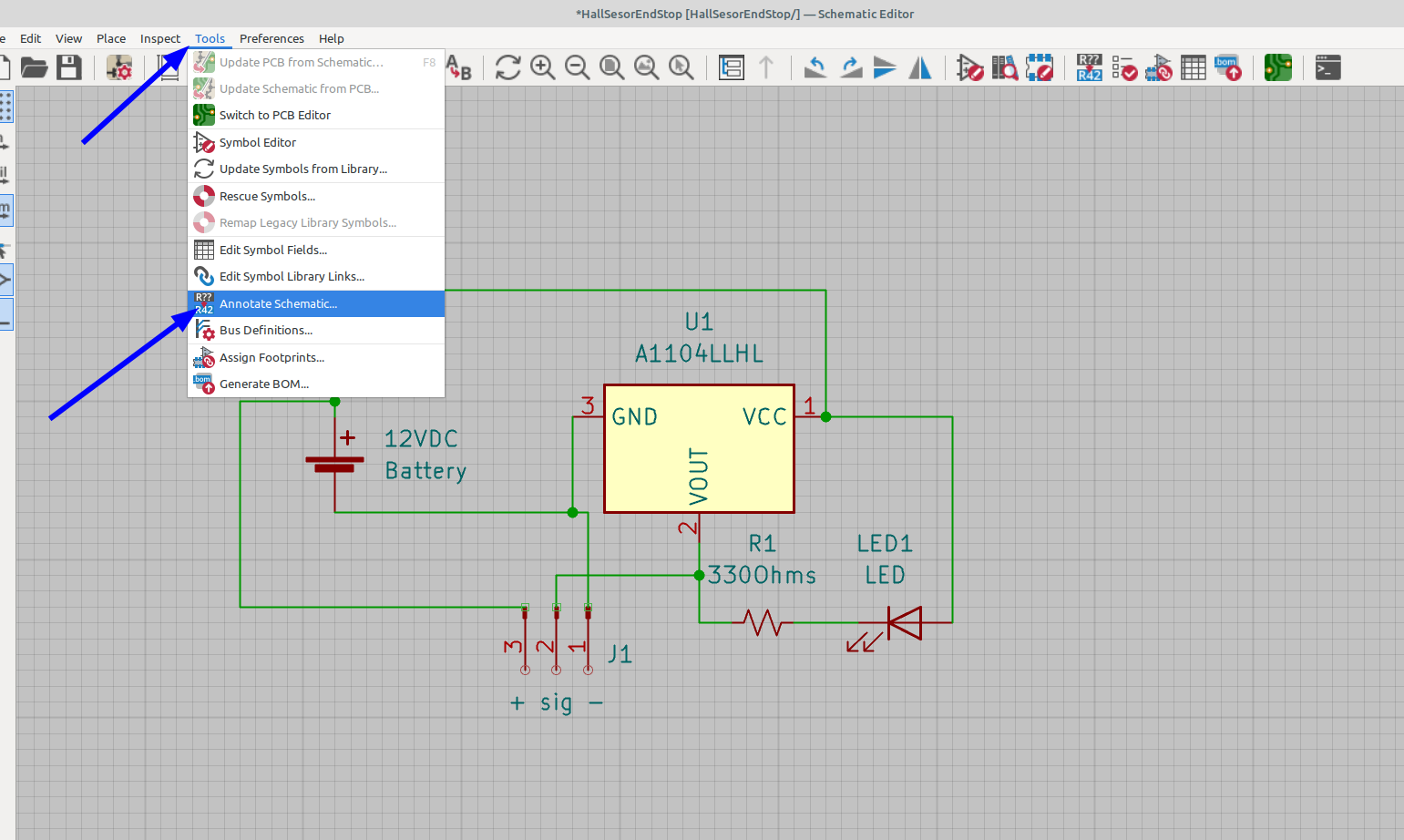
once everything is wired up then you need to annotate the schematic so when the netlist is exported everything is properly labelled and the schematic matches the pcb, go to Tools>Annotate Schematic:
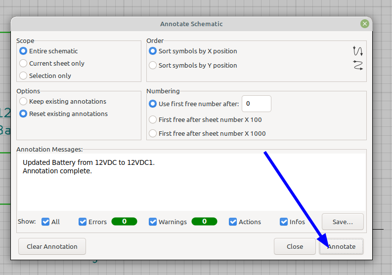
then click annotate and all of the descriptions will update:
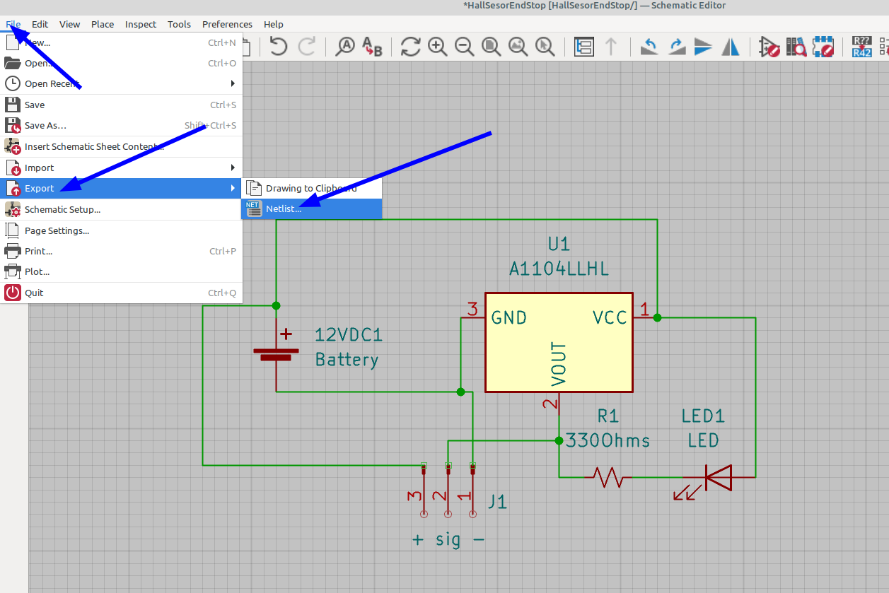
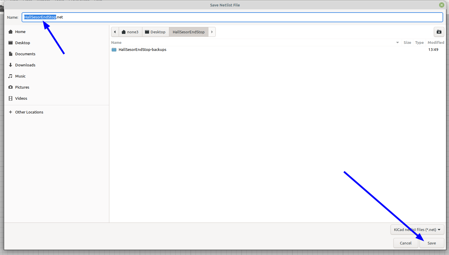
Now all that is left is to export the netlist so it can be imported into the pcb editor to design the circuit board:
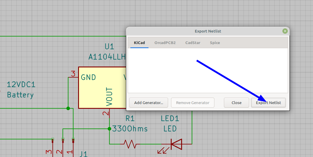
It should automatically save to the working folder for the project:
And that's it we are now ready to start a new PCB and make a circuit board, in the next part I will got through the netlist import process, placing components on the board and changing things like the trace width, making a copper pour and editing the drill and pad sizes.