
3D part design with Inkscape and OpenSCAD #58: Using KiCad, OpenScad and InkScape to make a solder free 3D printed circuit board.
A method to make a printed circuit board with a 3d printer.
After making the pcb stencil in part 27 I decided to use the same method to make an entire circuit board that I could use conductive epoxy to make a functional 3d printed circuit board, here are the steps I used.
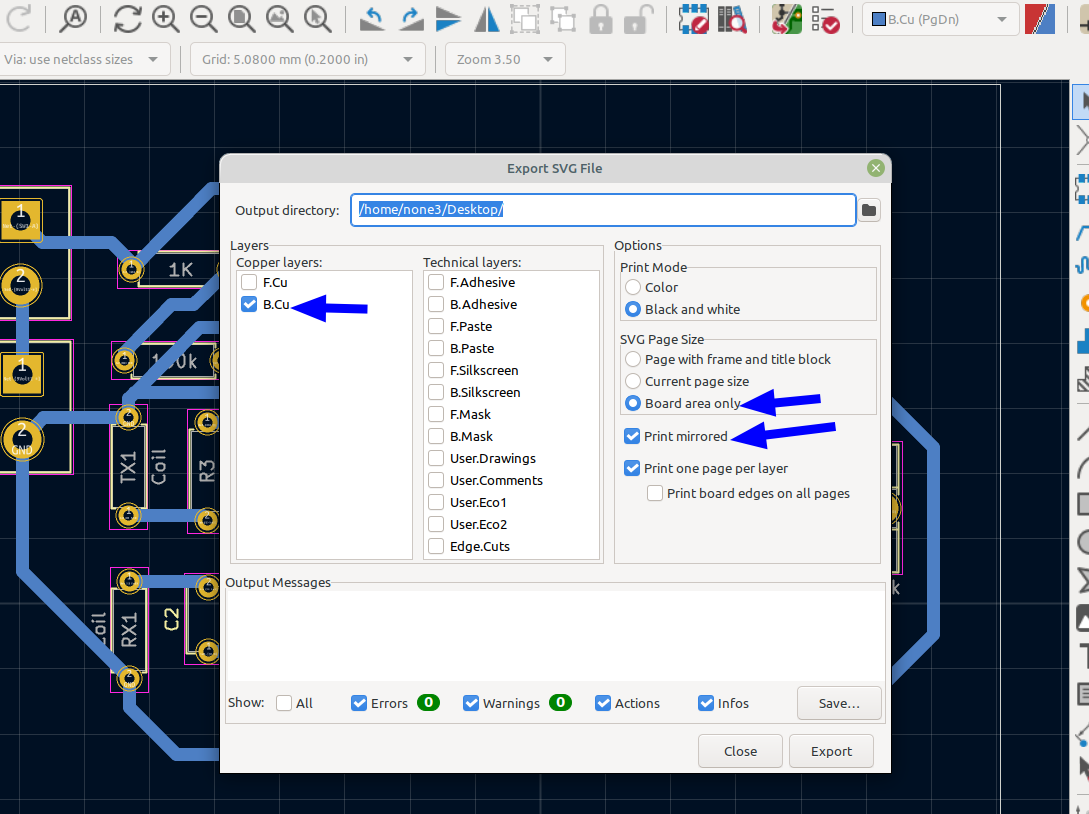
Step one > export an .svg file of your board from KiCad:
File>Export>SVG
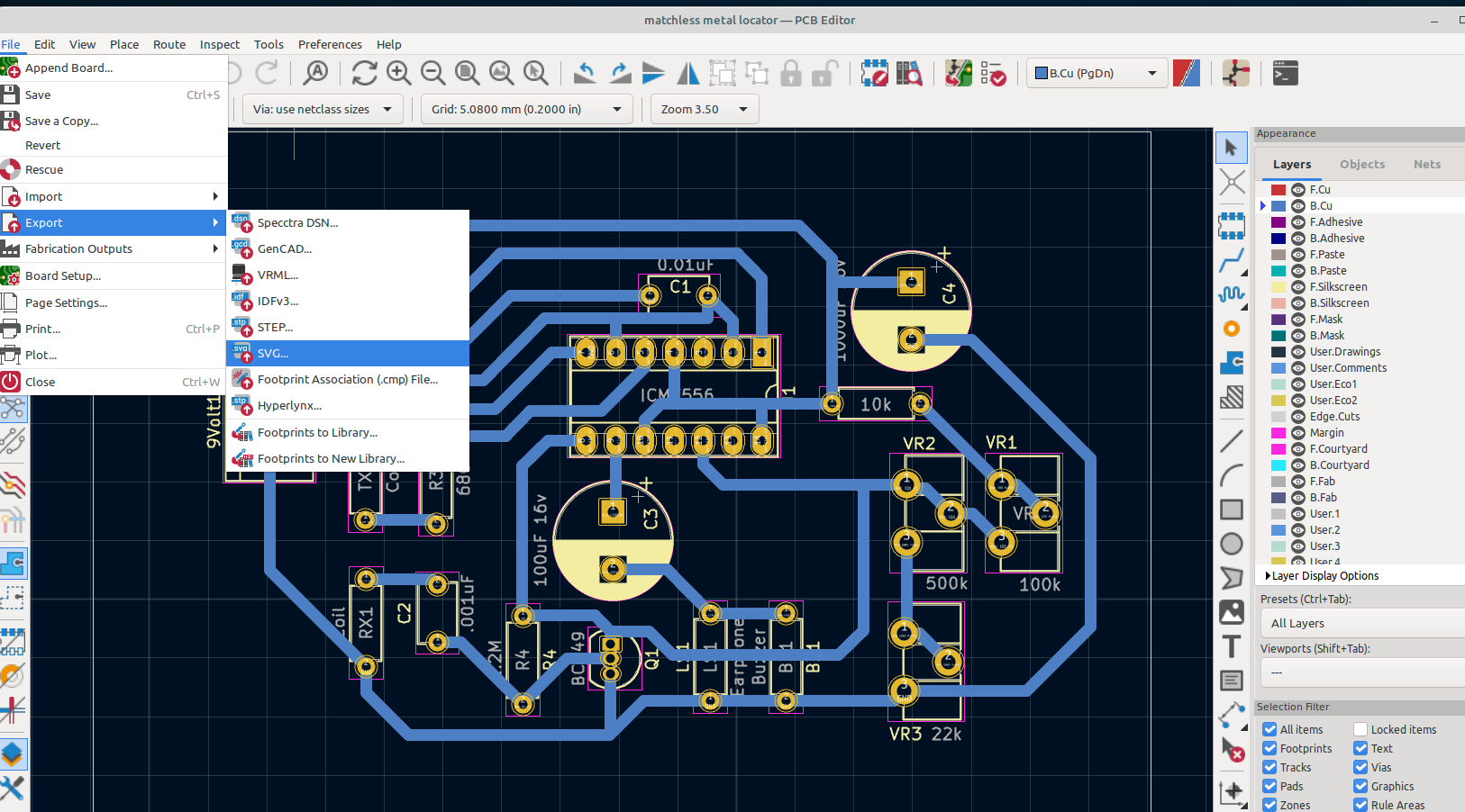
For this example I am using the bottom copper layer with through hole components:
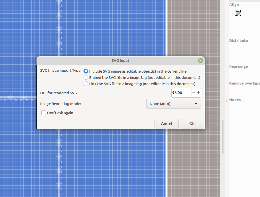
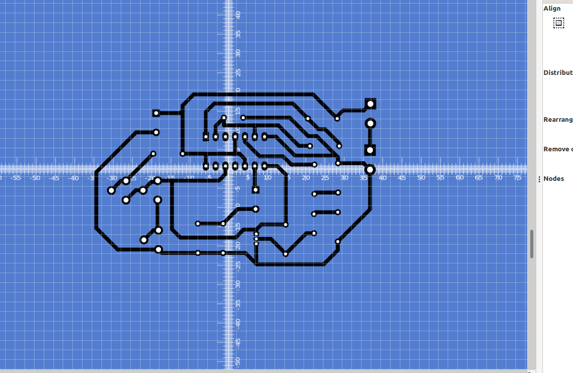
Once you have saved the svg file, then you can import it into Inkscape:
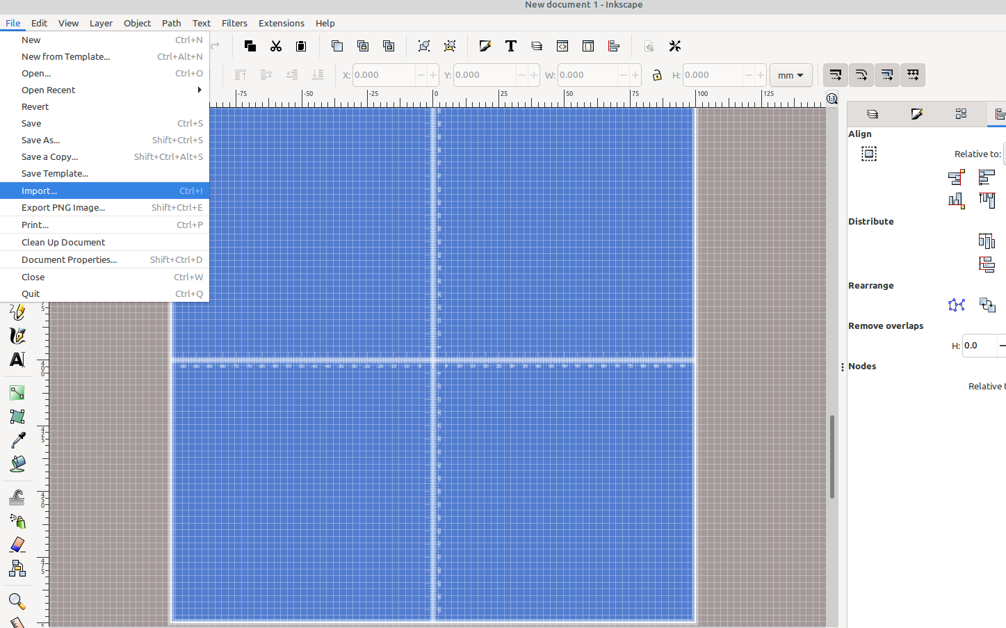
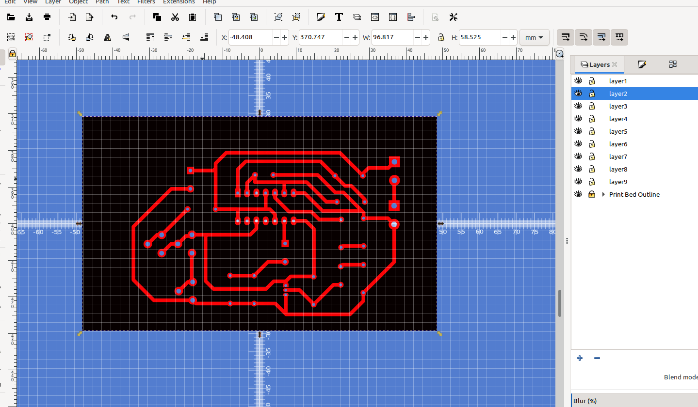
Once it is in InkScape it should look like this with drill holes, pads and traces:
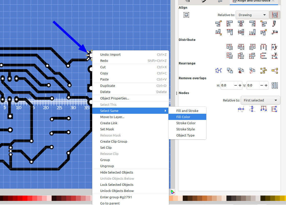
You should be able to select one of the white circles (drill holes) then right click on it and go to Select Same> Fill Color
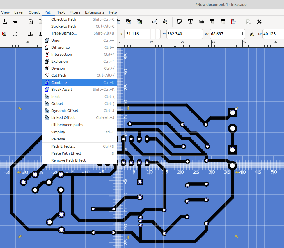
Now all of the white circles should be selected, then go to Path> Combine which will combine all of the white circles so we can use them to cut holes in a layer for our through holes:
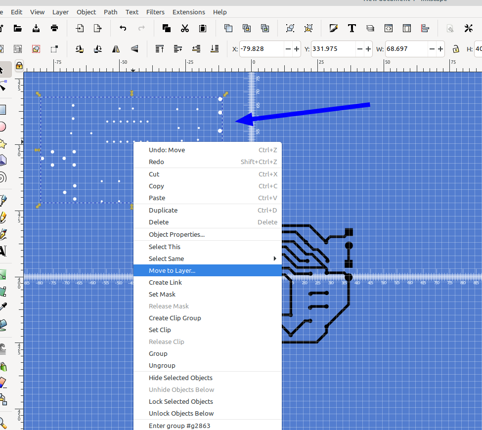
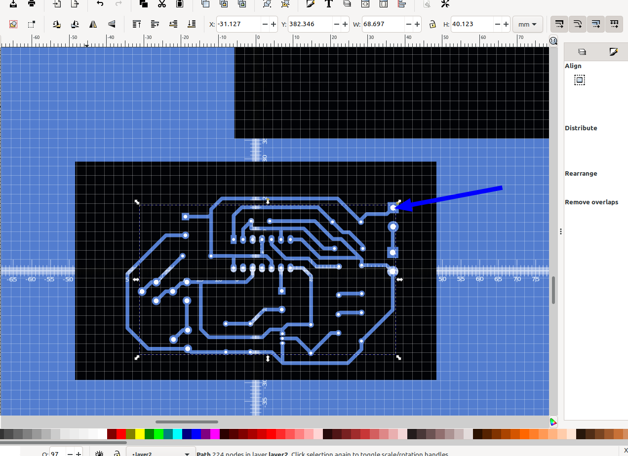
Next select the drill holes, move them away from the pads and traces, right click and move them to layer 2:
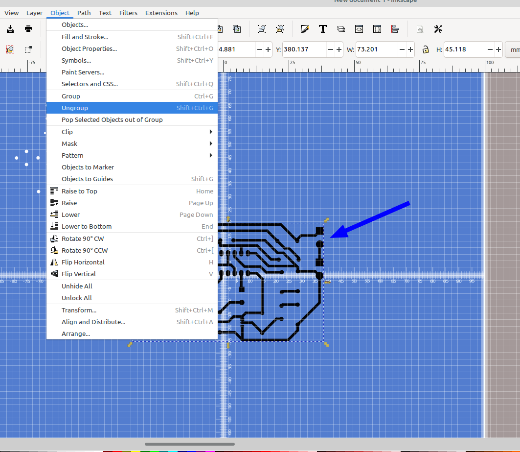
Next select all of the pads and traces and go to Object> Ungroup:
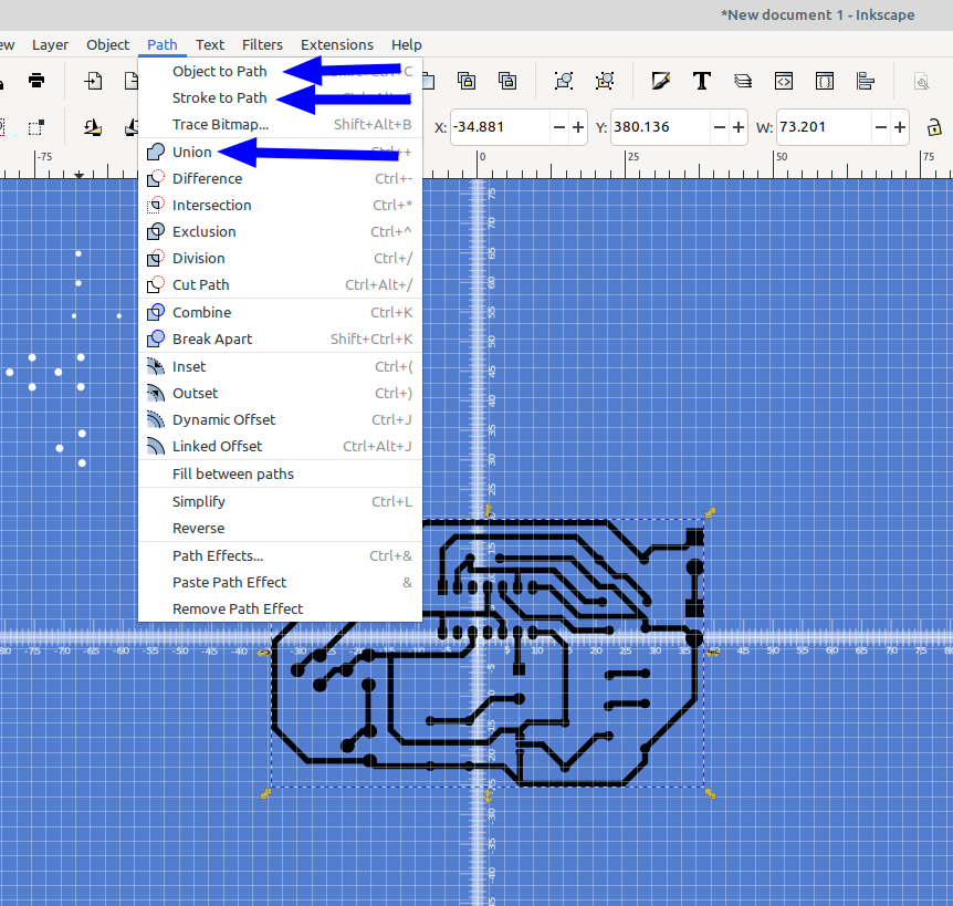
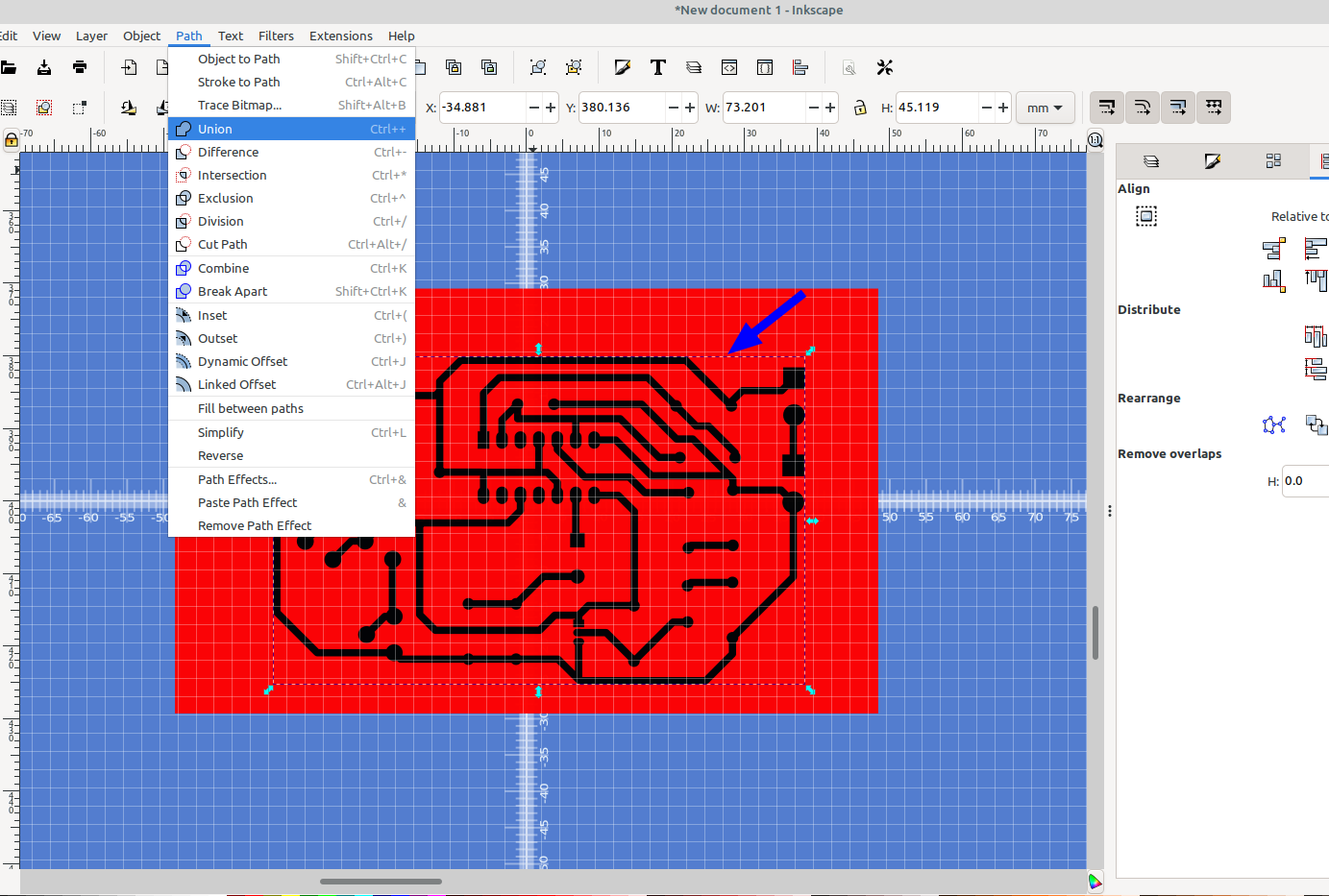
Then select all of the pads and traces again and go to Path> Object to Path, then Stroke to Path, then Union. This makes sure they will all act as one path when we use difference to make the traces on the board:
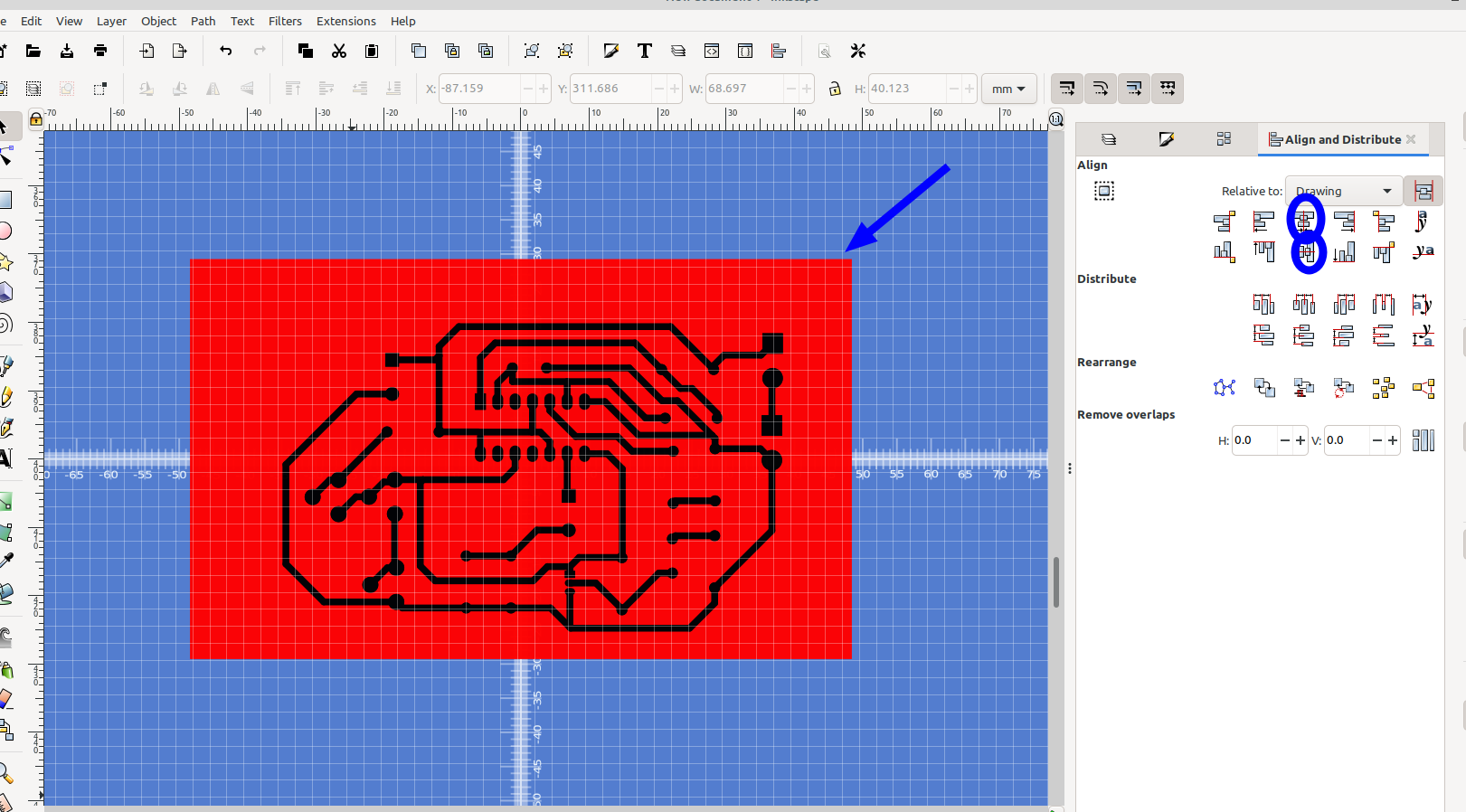
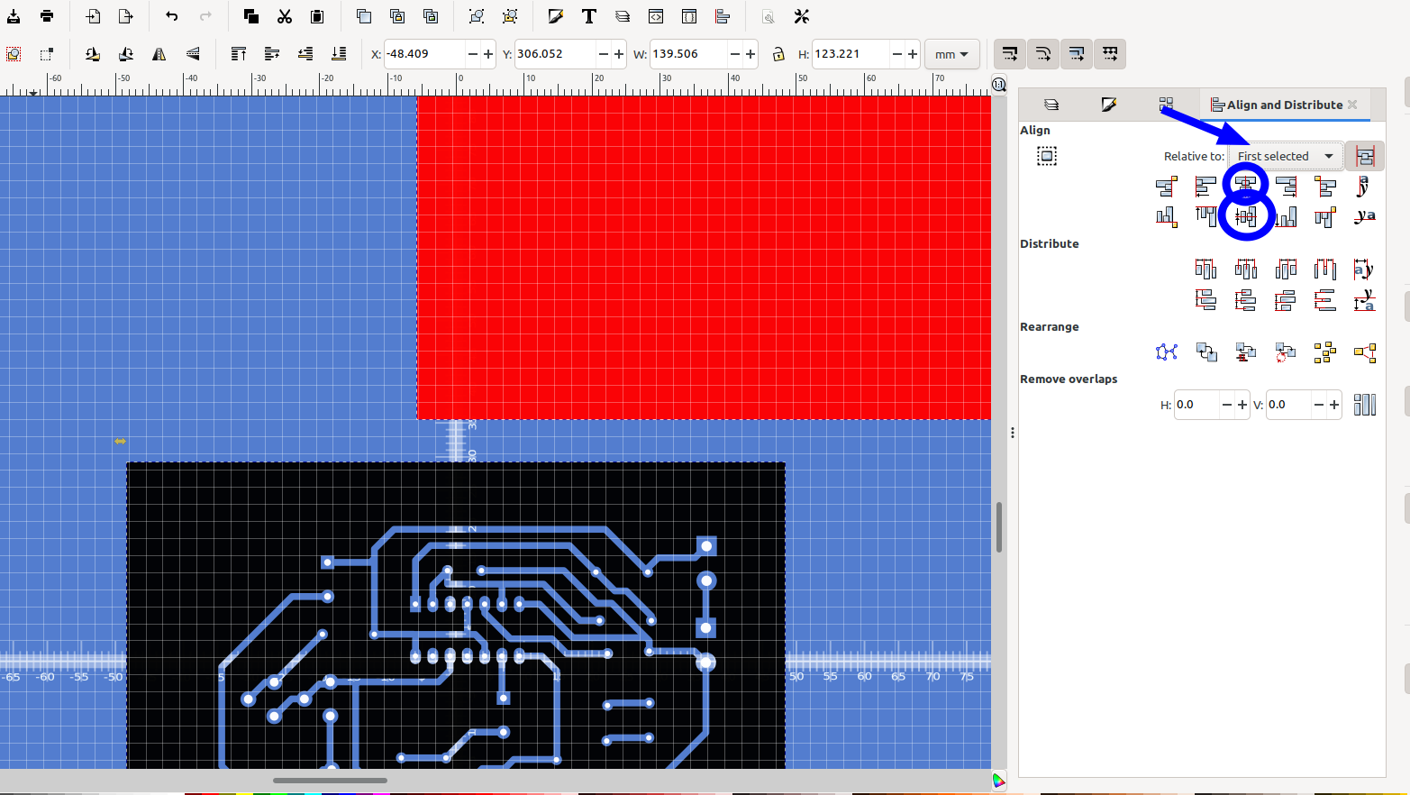
Next draw a rectangle the size you want the board to be and center it to the drawing with Align and distribute, I made it red so it's easy to see the traces, you may need to go to Object> Lower to get the rectangle on the bottom of the traces:
Then select the traces and use align and distribute to center them on the drawing :
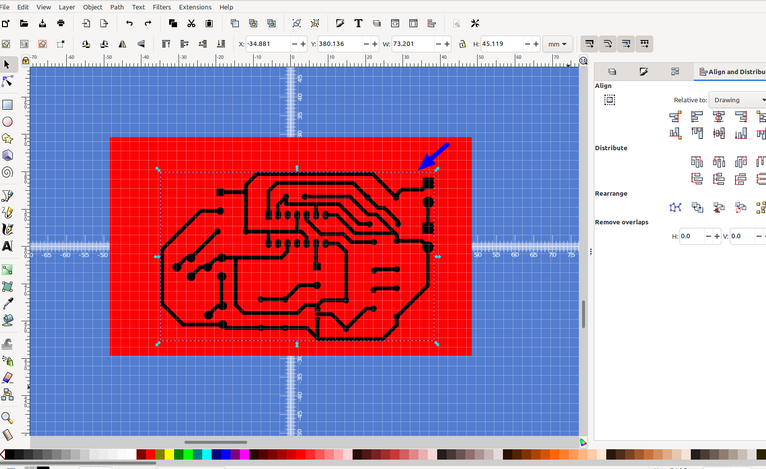
Then select the traces again right click and choose Select Same>Fill Color:
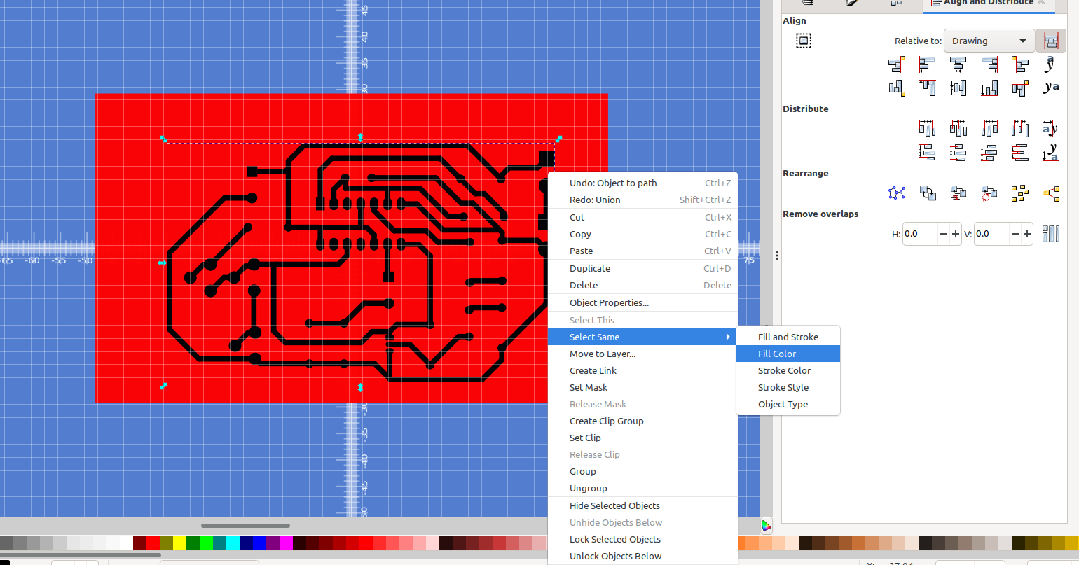
All of the pads and traces should have highlights around them:
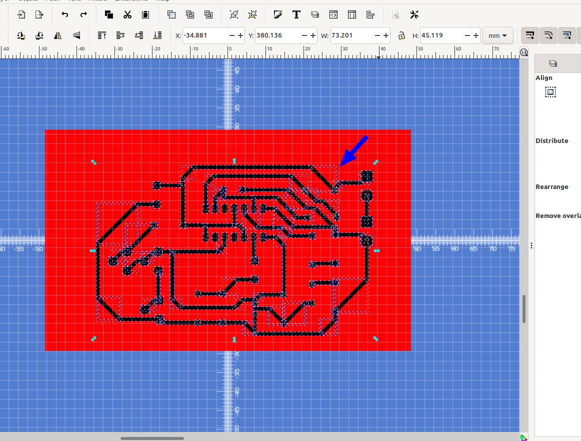
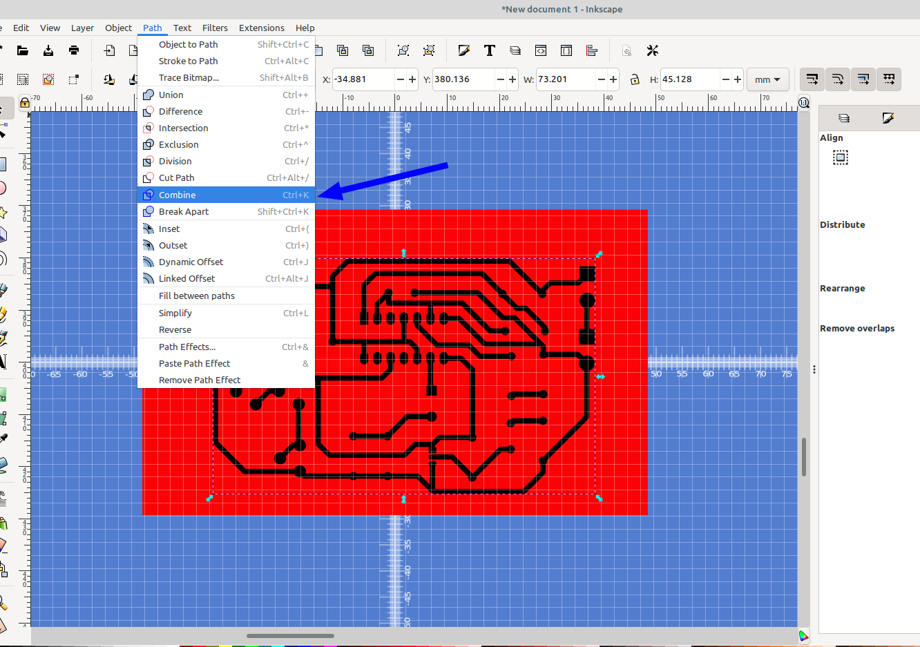
Now go to Path> Union:
And then Path>Combine
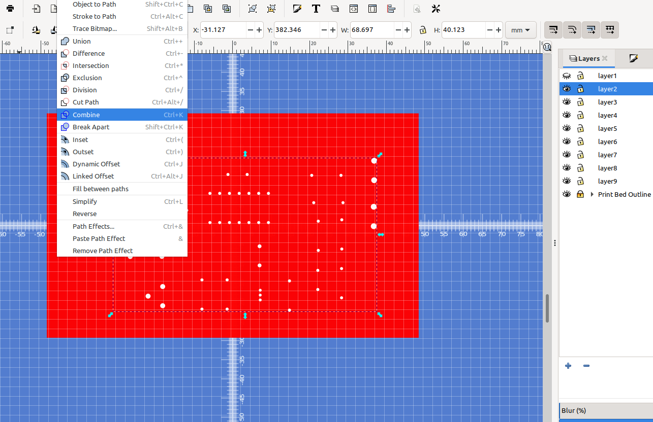
Next select the red rectangle, copy and paste it, drag it out of the way and move it to layer 2:
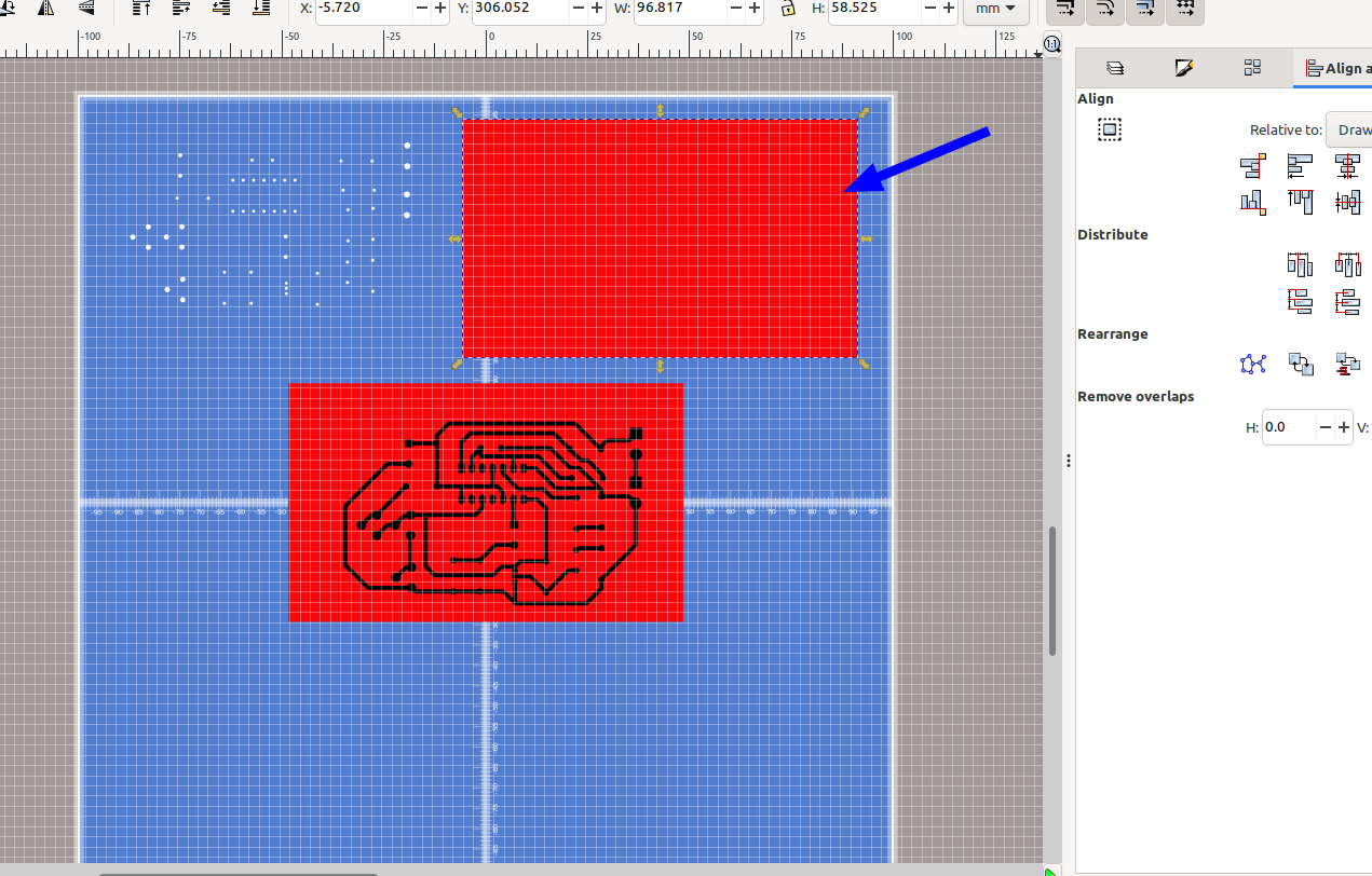
Next select the pads and traces, hold down shift and select the red rectangle> both patterns should have a highlight around them, the go to Path> Combine:
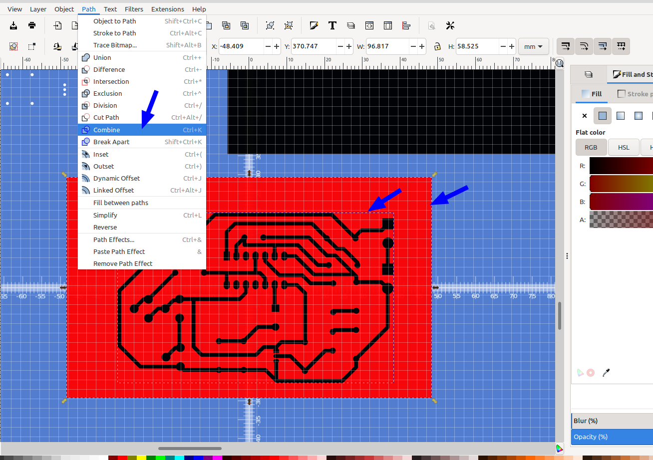
Now you should have a black rectangle with the traces subtracted from it. I tried several different ways to get the traces to subtract from the rectangle as a group, the above steps were the only way I could get it to work properly due to the complexity of the shape.
Next select the white drill holes and align them to the traces that were just cut out, as long as they are highlighted you can use the arrow keys on the keyboard to align them perfectly with the pads:
Next select the black rectangle with the traces, hold down shift and select the red rectangle, then align by first selected and center them:
Now select the white drill holes and go to Path> Combine:
Note you may need to lower the red rectangle if it is on top of the white drill holes and you can't see them.
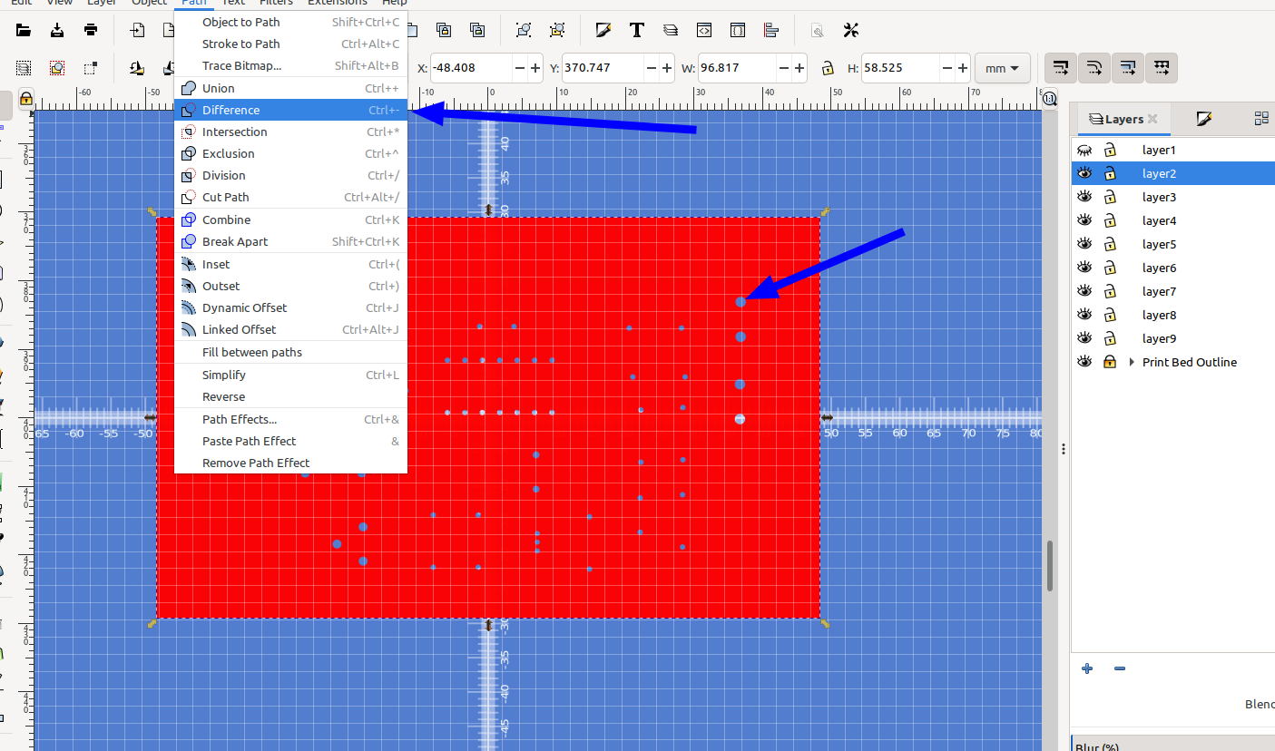
Next select the white drill holes, hold down shift and select the red rectangle, then go to Path>Difference. You should have holes in the rectangle for the drill holes now
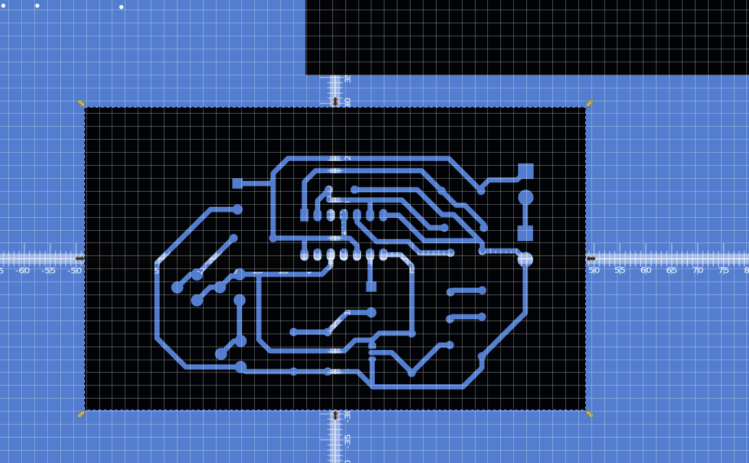
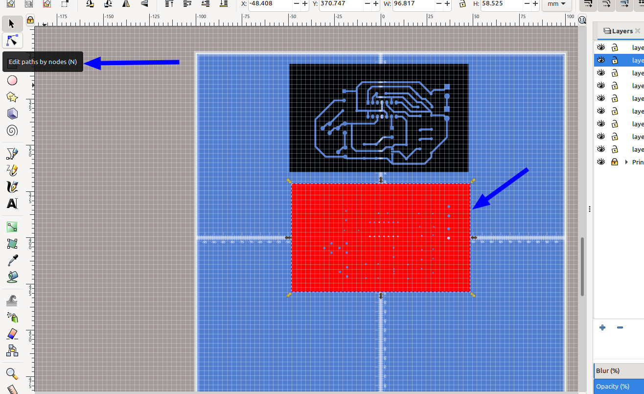
Now if you align the two rectangles you should see something like this with the traces on layer 1 and the drill holes on layer 2:
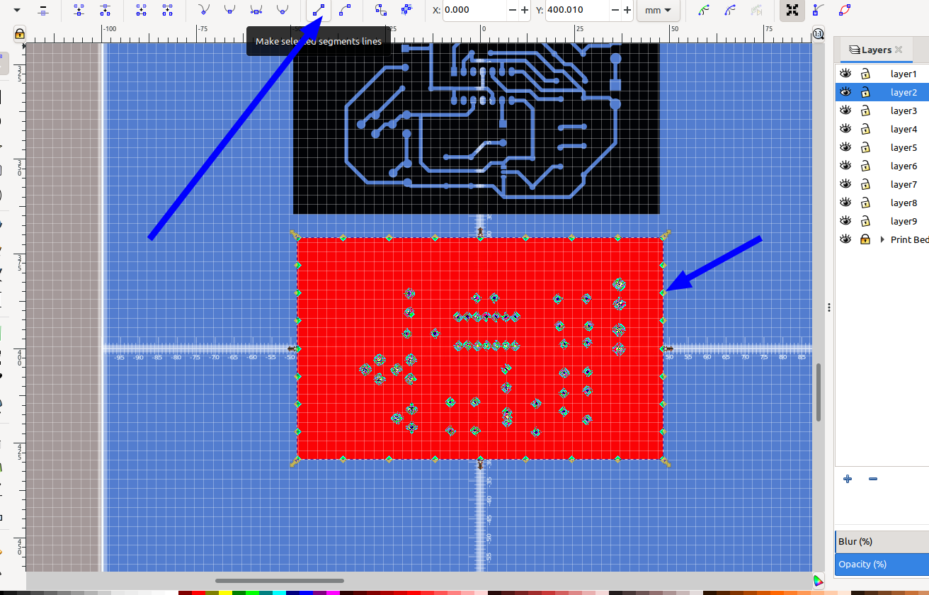
Next separate the two rectangles, select the red rectangle and select edit paths by nodes in the left hand menu:
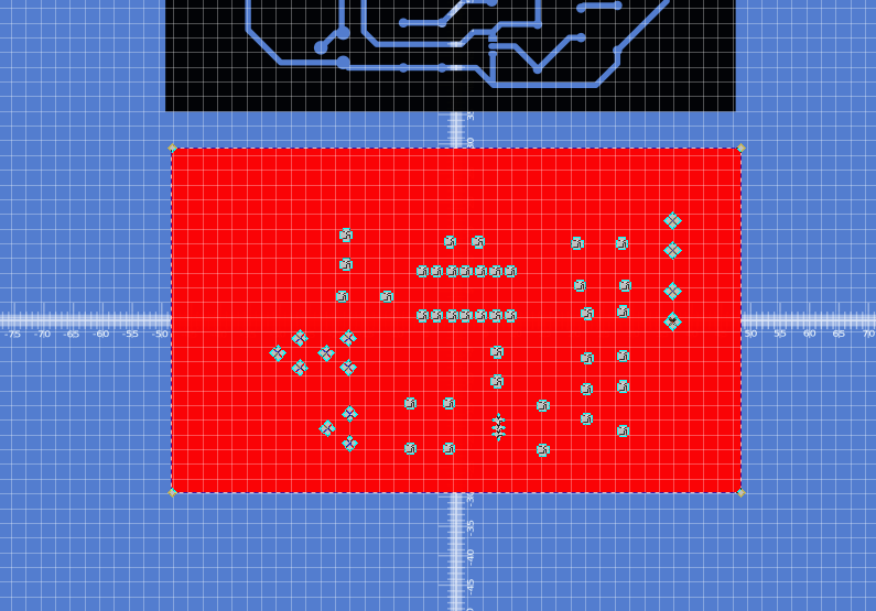
The red rectangle should have highlights around the outside and the holes, using the mouse click and drag to select the object again, the highlights will change color indicating all of the nodes are selected:
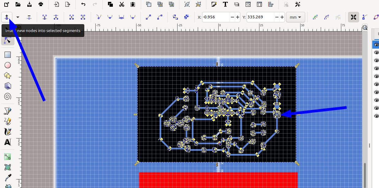
Next add new nodes by clicking the add nodes icon three times:
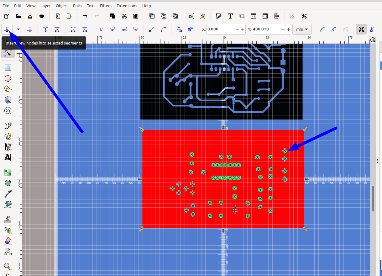
And convert the segments to lines:
Next do the same for the traces:
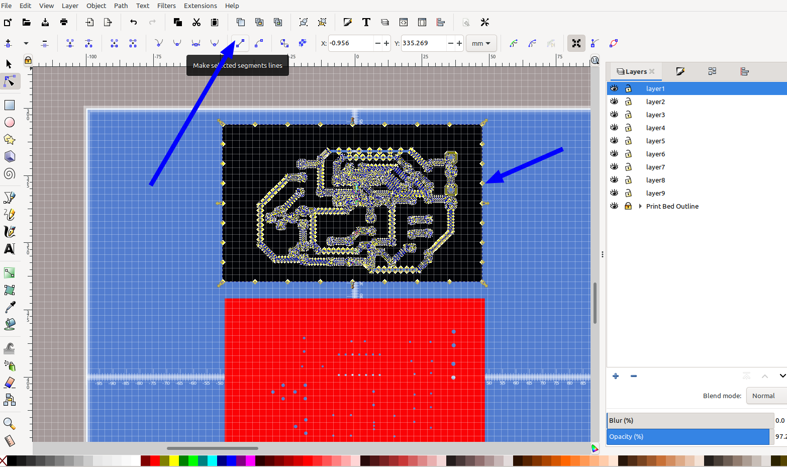
then center the two rectangles on the center of the drawing again by using align and distrubute:
I am using the custom print bed template that I made for InkScape:
 Bob
Bob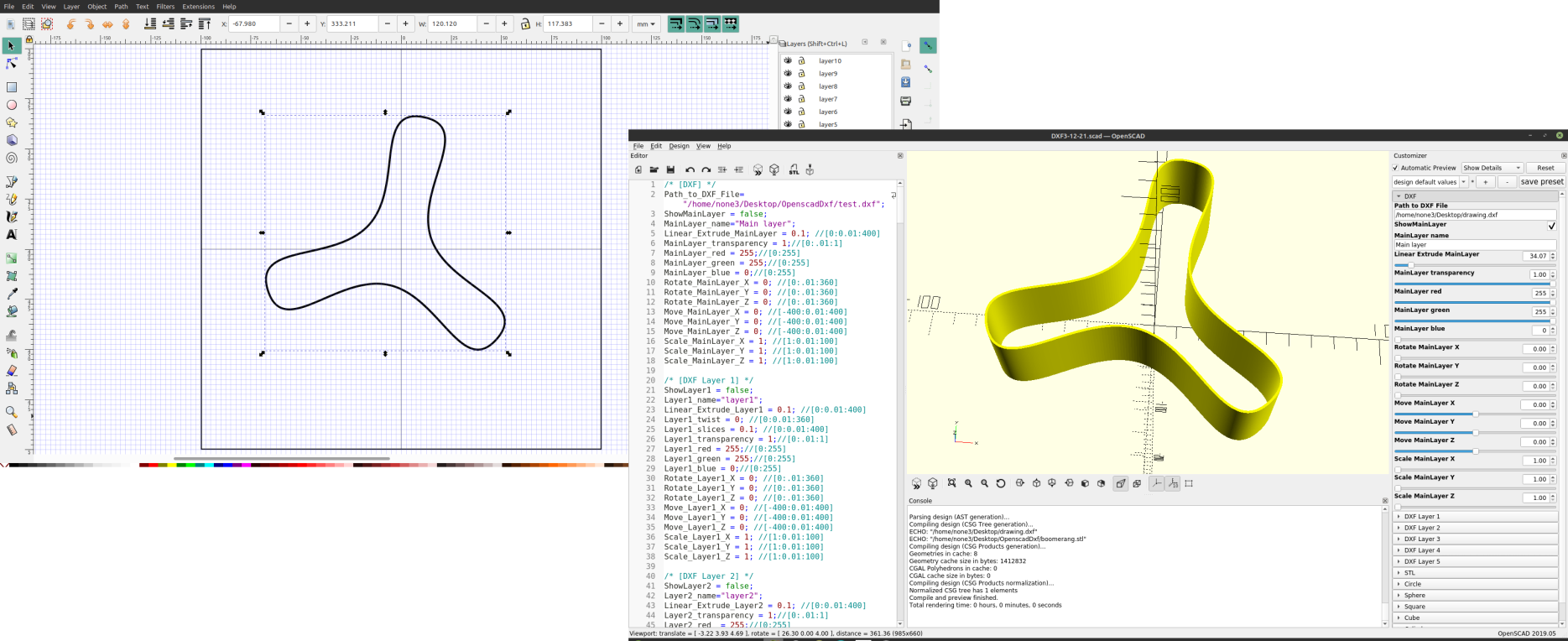 Bob
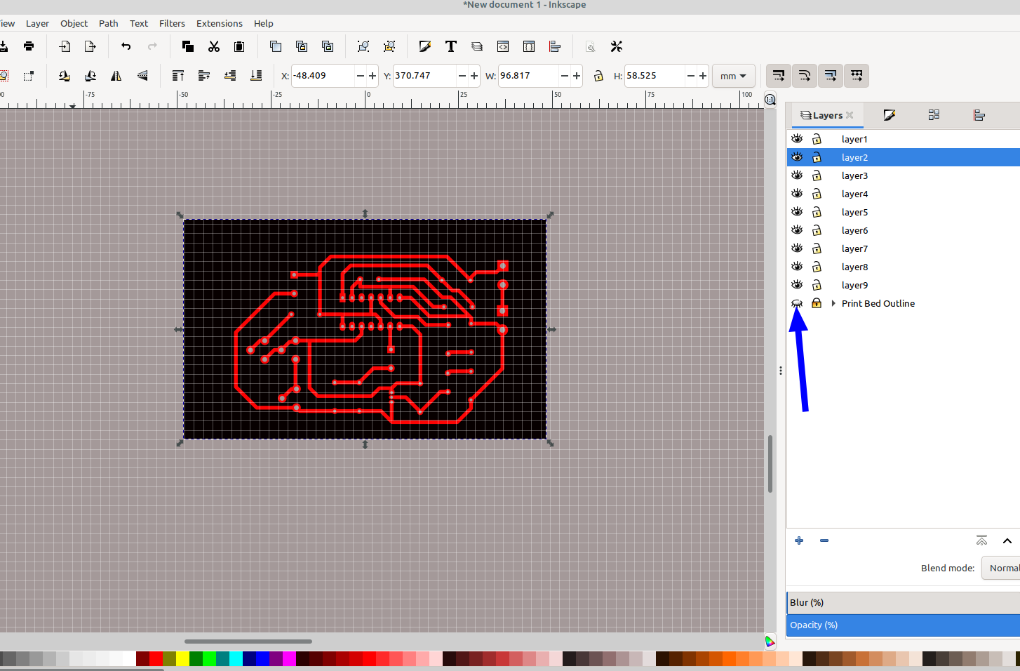
Bob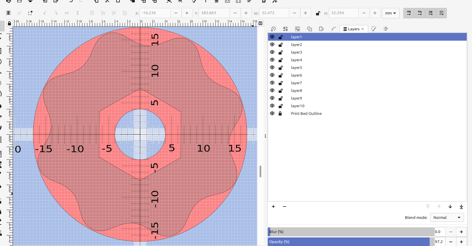
I hide the print bed outline layer before I export the file to DXF , if you aren't using a custom template just make sure you hide anything you don't want exported.
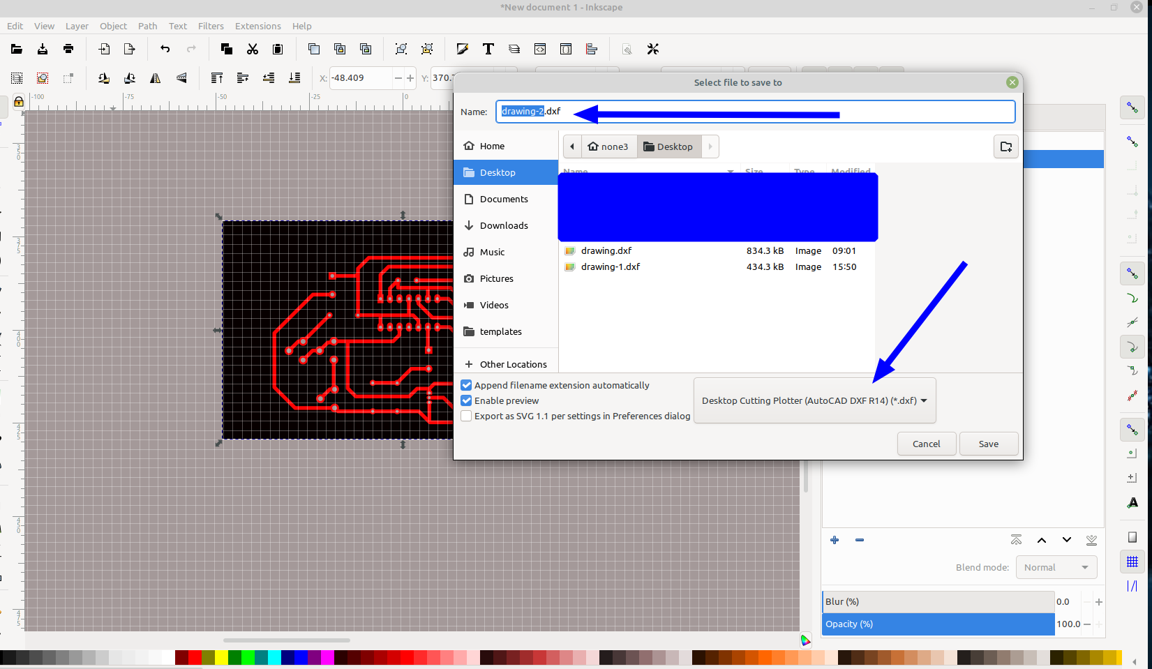
Then go to File> Save as:
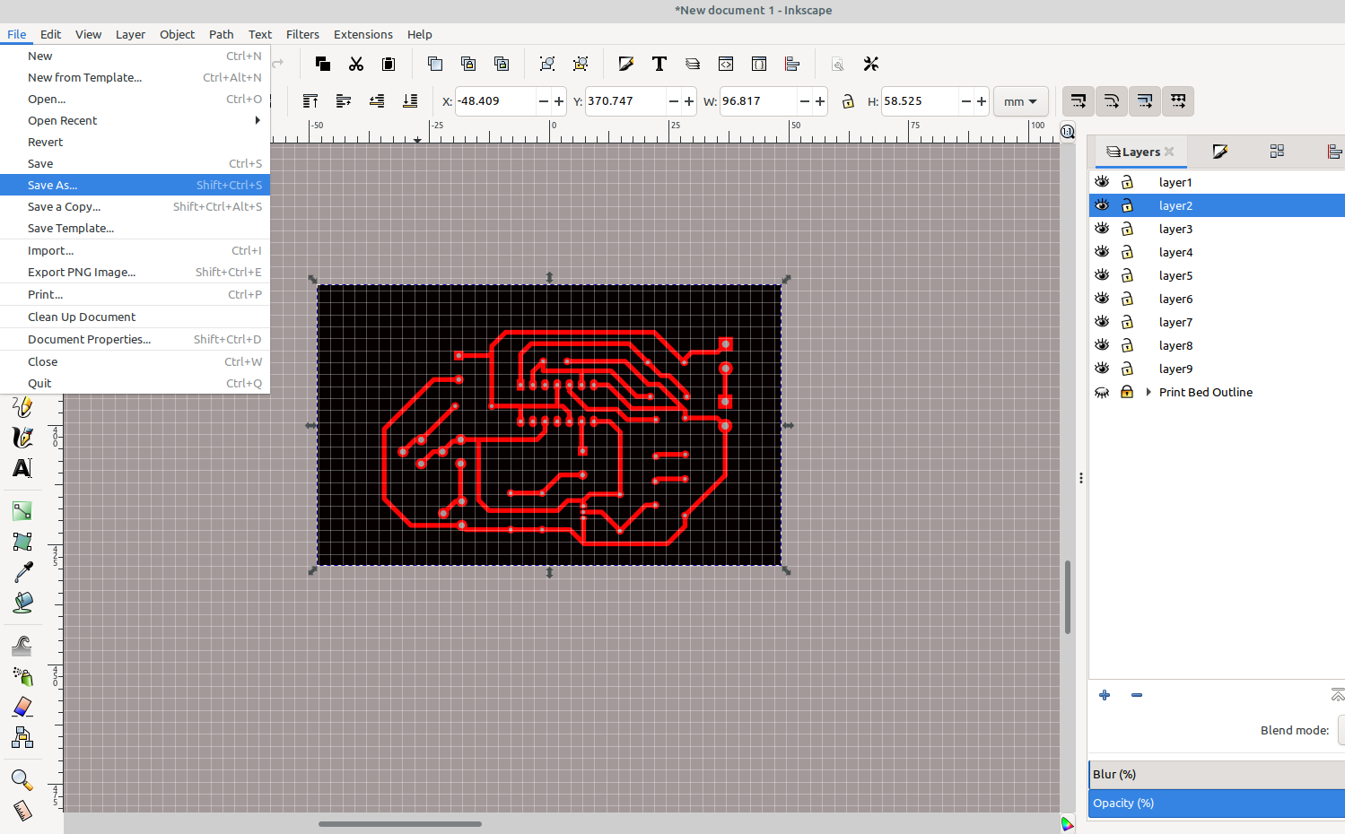
And save your file as a DXF 14 file so it can be imported into OpenScad
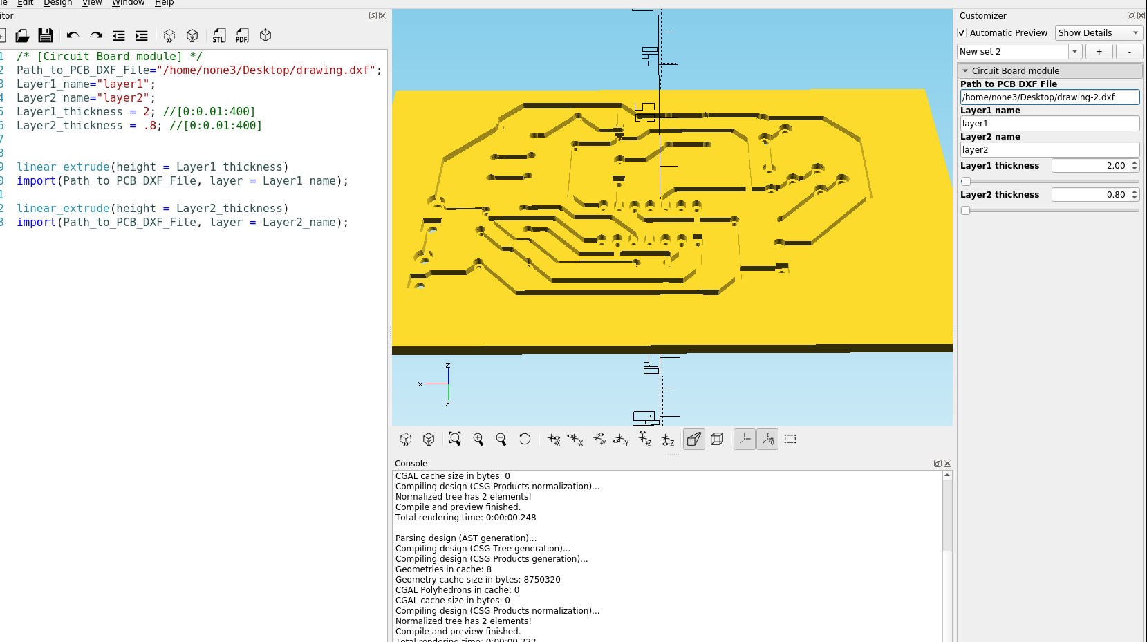
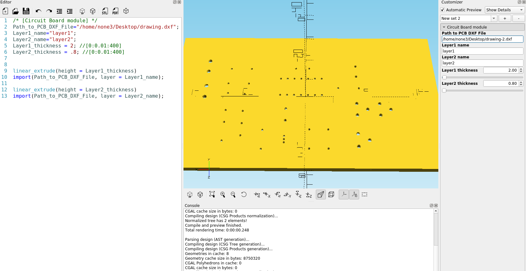
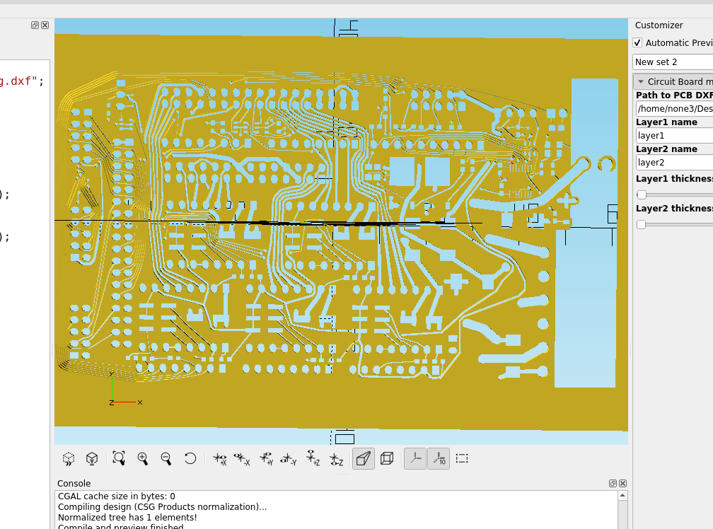
Now that it is saved we can import it into OpenScad, I made a module that makes it easy to adjust the size of the layers, here's the code:
/* [Circuit Board module] */
Path_to_PCB_DXF_File="/home/none3/Desktop/drawing.dxf";
Layer1_name="layer1";
Layer2_name="layer2";
Layer1_thickness = 2; //[0:0.01:400]
Layer2_thickness = .8; //[0:0.01:400]

linear_extrude(height = Layer1_thickness)
import(Path_to_PCB_DXF_File, layer = Layer1_name);

linear_extrude(height = Layer2_thickness)
import(Path_to_PCB_DXF_File, layer = Layer2_name);
Just change the "path" to where you saved the file on your machine, alternatively you can just comment out the two imports and drag and drop your DXF into OpenScad in their place.
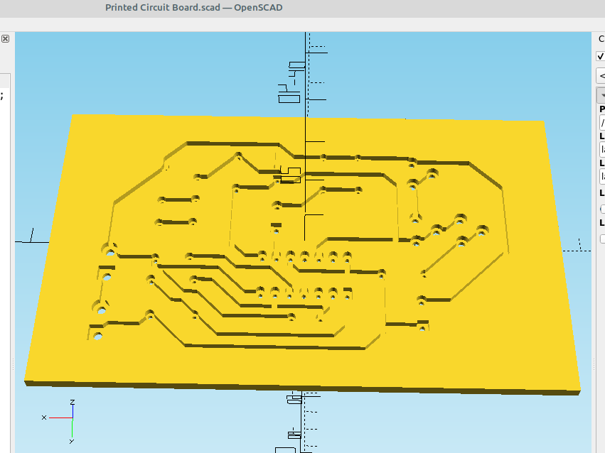
Now you can see that we have a drill hole layer that we can mount our components on and a layer that forms channels that we can use to pour conductive epoxy into to make the traces< I am working on a way to make some conductive epoxy that is showing some good results and I will be posting a part 2 of this that will go through steps on how to make it.
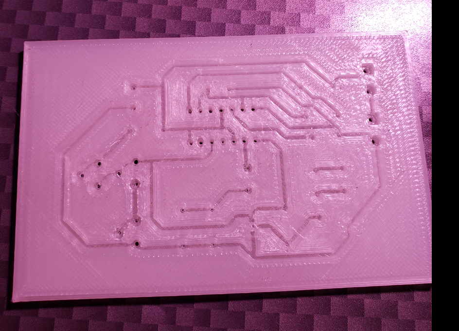
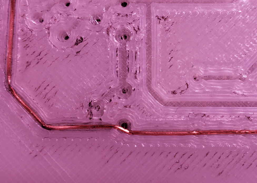
Using some copper wire salvaged from some cat 5 cable it's not too hard to make some copper traces that could be soldered , a 1.2 mm track width gives enough room to form the wire in the tracks and some super glue in spots helps hold it in place, the channels on this board could have been a bit deeper, and I'm sure an automatic tool that routes the wire could be made for a 3d printer pretty easily but doing it by hand isn't very hard with the right tools, more experimentation will need to be done :
At first this might seem like a long process, but after just a few tries I was able to make a board that was ready to 3d print in about 10 minutes.
And although I haven't tried it yet I'm sure you can make a 2 layer with board pretty fine traces with an sla printer, here is a "nice ramps" board that I will be trying:
 NiceCircuits
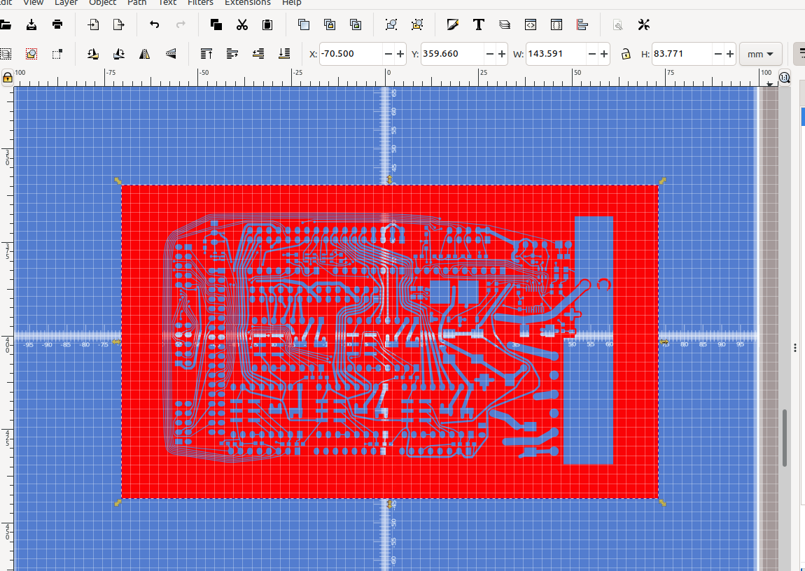
As always this is a work in progress and your results will vary, but it is an easy way to make a functioning circuit board with a 3d printer, and I will be improving on this as time goes by.