
Beginner's guide to designing a circuit with kicad 6.0 part 2: PCB editor
Part 2 of the beginner's guide to Kicad 6.0
After the schematic is made it's time to design the circuit board and here are the steps involved.
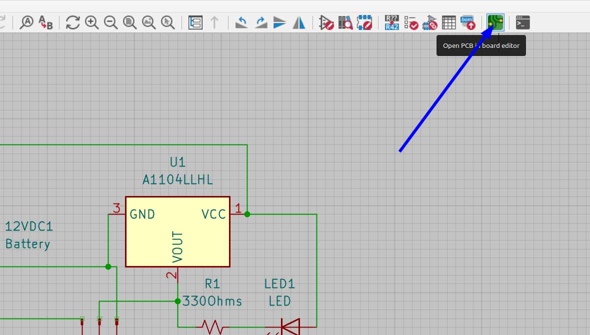
In the schematic editor window there is an icon to open the pcb board editor, click on it and the pcb board editing window pops up:
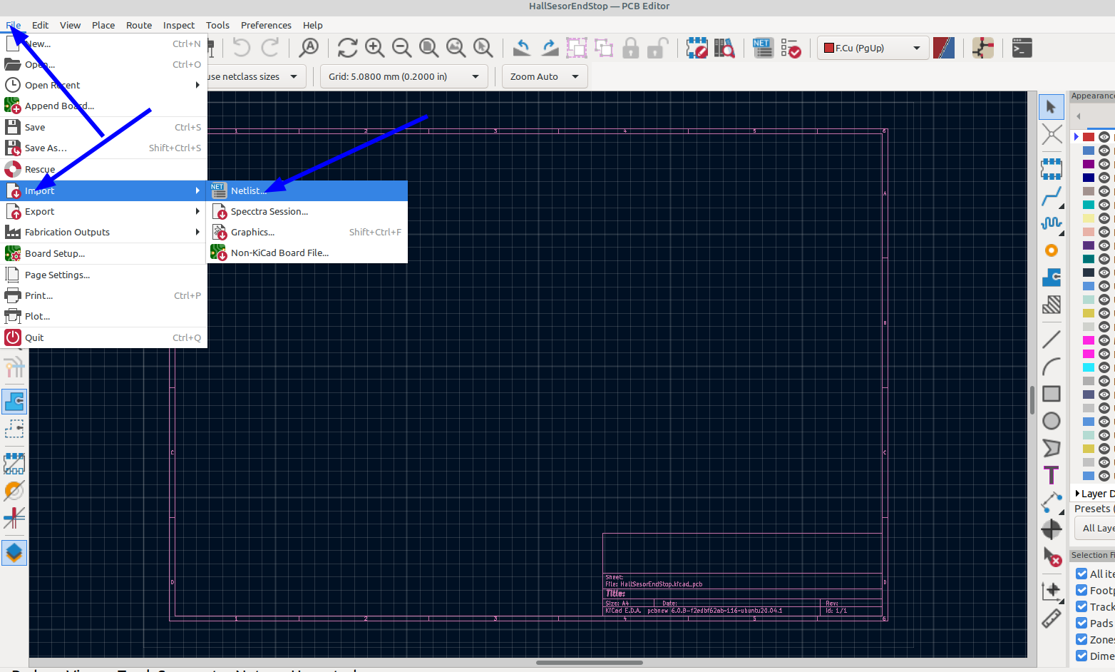
In the pcb board editor window go to File>Import> Netlist and import the netlist file we saved from the schematic:
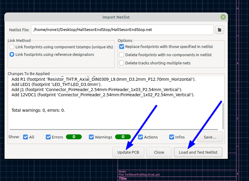
Click load and test netlist then update pcb:
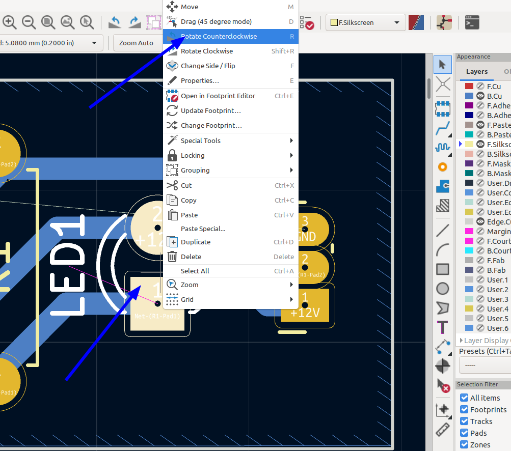
All of the components should show up outside of the sheet, you can select them and move them to the middle of the sheet and arrange them how you want them to sit on the sheet. By highlighting the component then right clicking a menu will popup to change the orientation of the components:
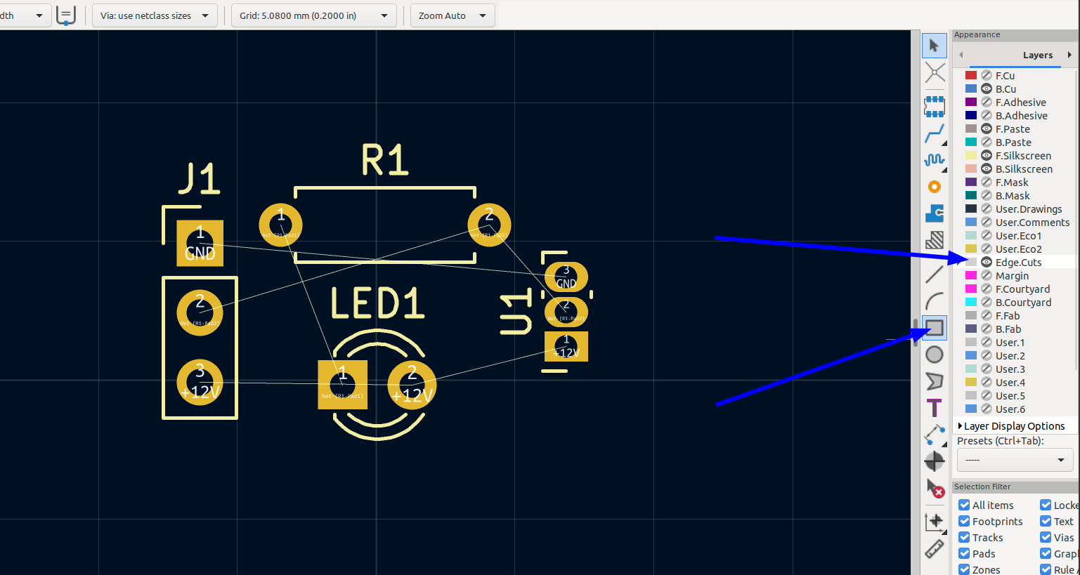
Once they are sitting how you want them you should make an outline on the edge cuts layer for the outline of the board, highlight the edge cuts layer and select the rectangle tool to draw a rectangle around the components the size you want your board to be:
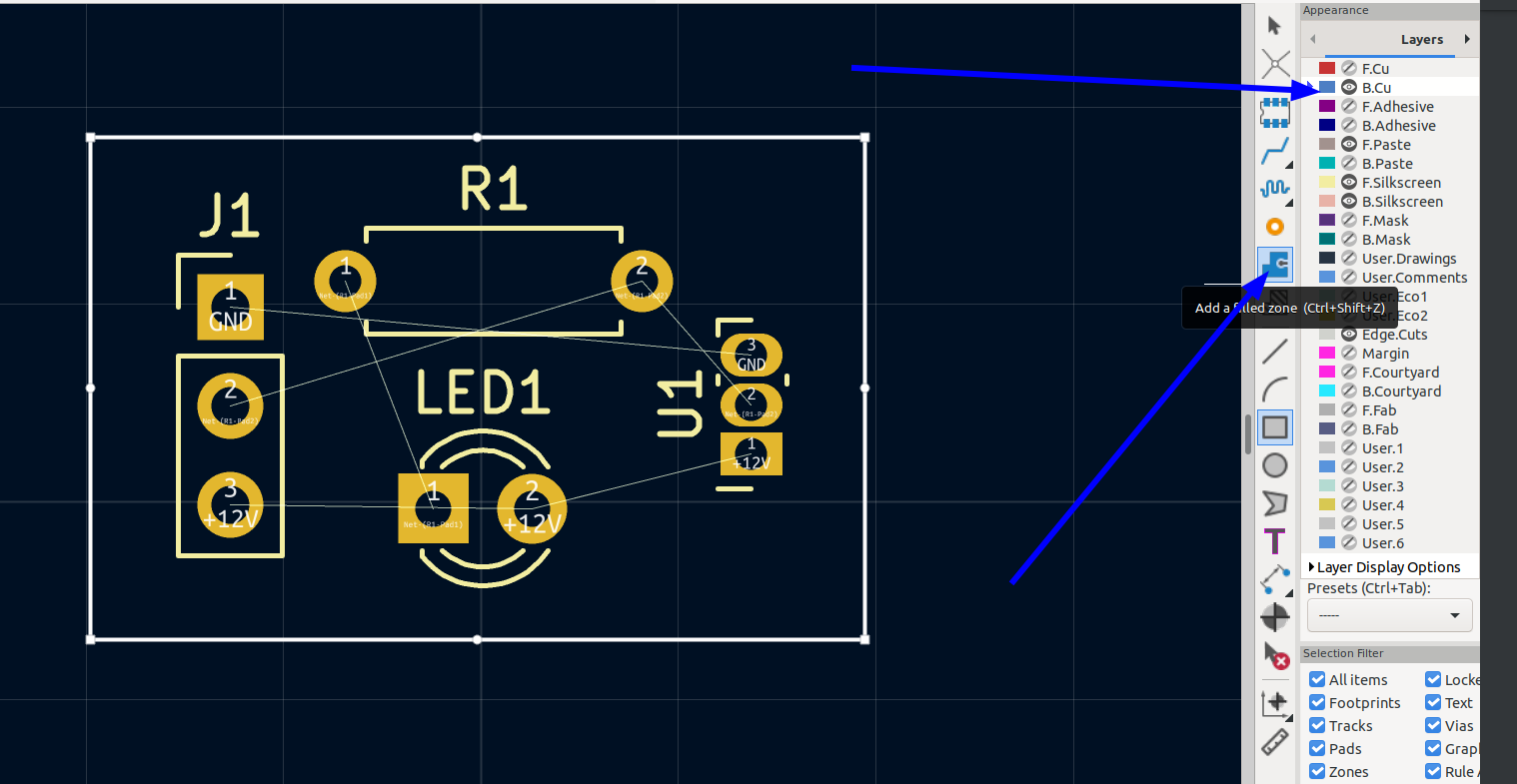
Next we are going to make the copper pour for the ground plane, this will fill most of the board with a copper plane for the ground connections.
Highlight the copper layer you want the ground plane to be on and then select add a filled zone:
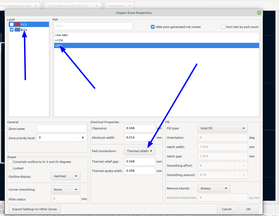
A properties page will pop up and you can assign witch layer you want the zone on, the clearance from the tracks, type of pad connections, fill type, etc.
Now you can draw the ground plane where you want it on the board, I made mine fill pretty much the whole board but you can make it only in a specific area if needed. When you are done drawing the shape for the plane, right click on the add a filled zone icon, select fill all zones and the filled zone will show up :
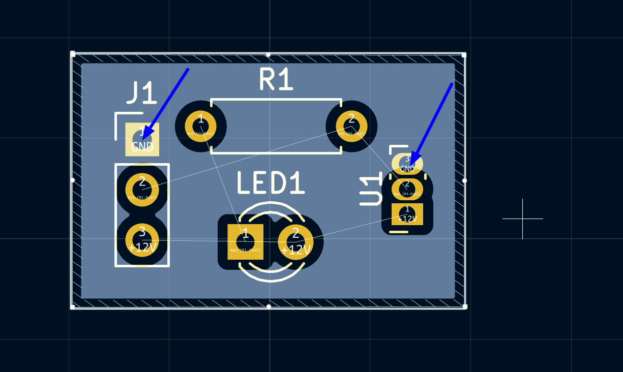
Notice that anywhere we have a ground connection the pad is connected to the ground plane, this greatly reduces the number of tracks needed:
Now we can route the traces that connect the components together, click on the route tracks icon and click on the end of a component, then route the traces between the components. This is a simple board so routing the traces is easy, on more complex circuits a multi layer board is needed, but the more you route tracks the better you get at it , proper component placement is the key.
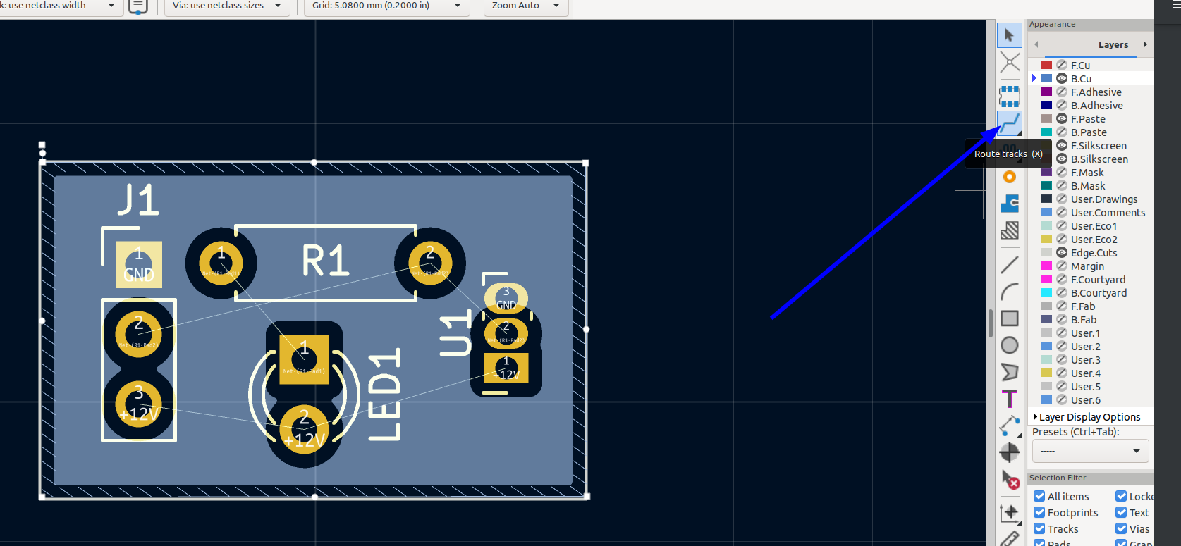
You will notice the light yellow lines connecting the components these show where the traces need to connect to each component, as you connect everything together you will see how they work. When you first start out there are some things that will make building a board easier like making your traces wider and pads larger, making the traces wider makes them easier to etch and having larger pads makes drilling and soldering much easier. Nothing is worse than trying to solder pads that have no copper left around them and traces that are so small they break.
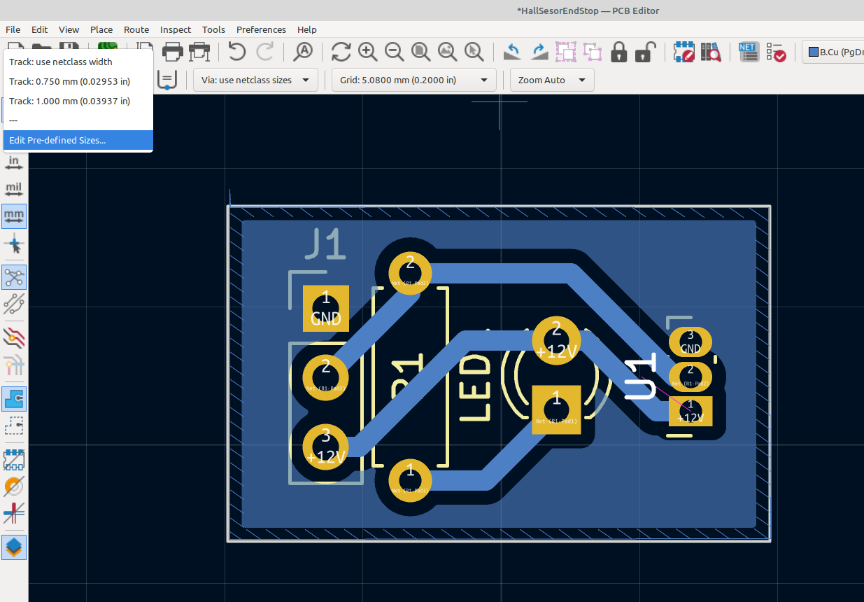
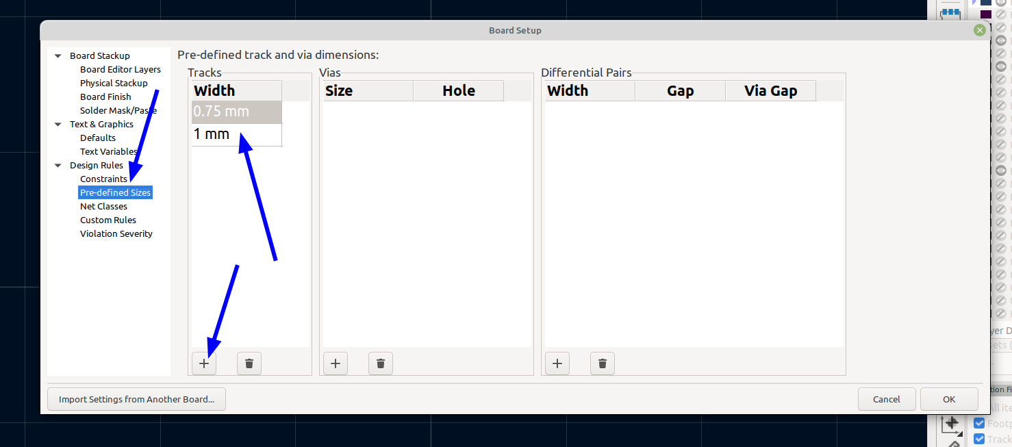
You can set the track width really easily in kicad, in the upper left hand corner there is a drop down box to select the track width you want to use and you can make custom track widths, I set up a couple that were .75 mm and 1mm wide:
Click on the plus sign and add the track sizes you want then just select it from the drop down list when you are routing your tracks:
Changing the pad size and drill hole diameter is pretty easy also, just select the pad you want to modify, right click and got to pad properties, then you can change all of the settings for the pad:
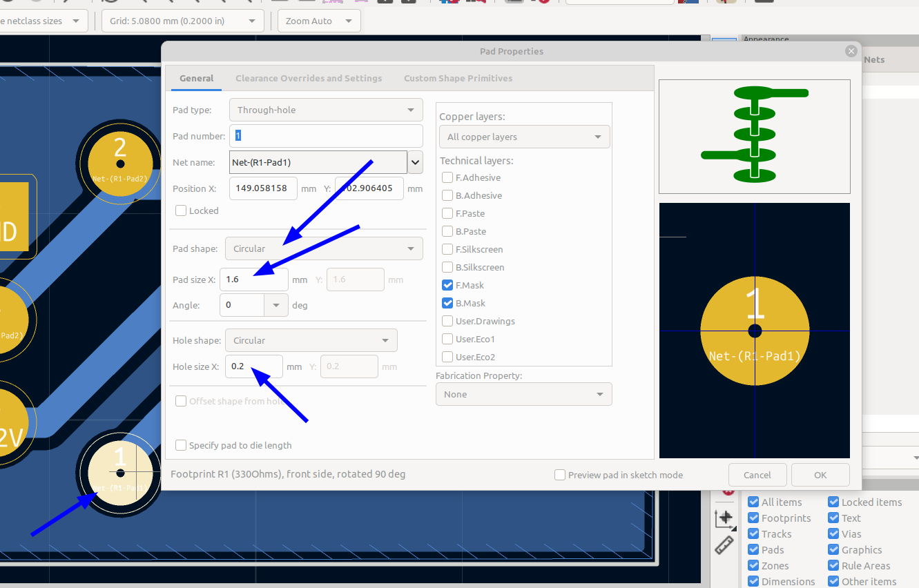
I will usually make the tracks and pads larger just to ensure I have a good board that's easy to drill and solder when it's all done.
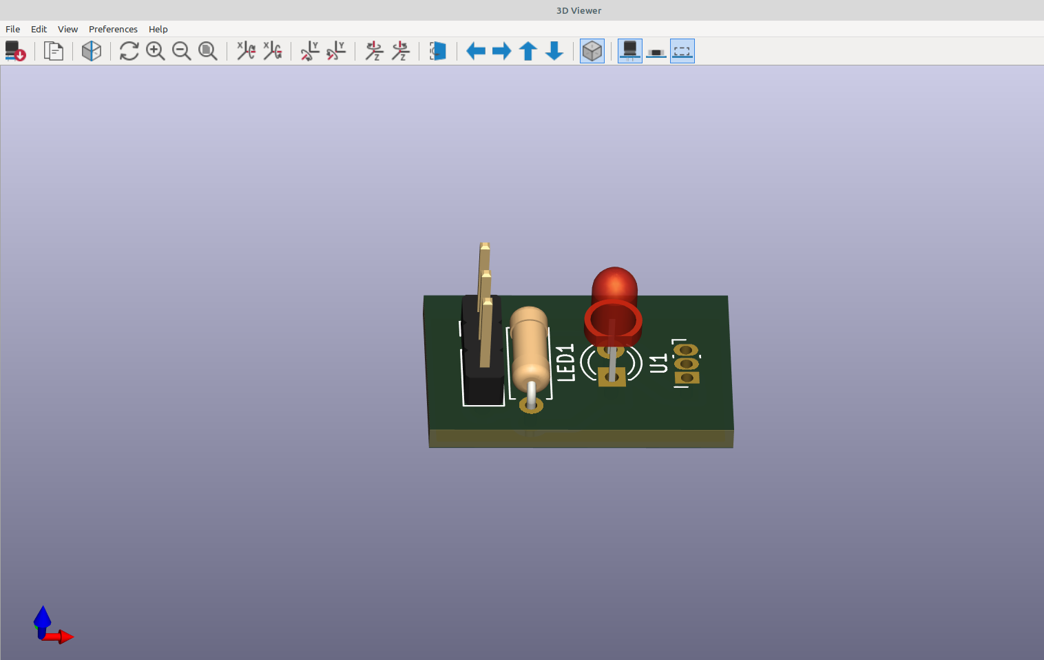
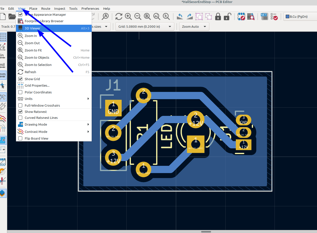
After everything is laid out and routed you can use view 3d to see how everything looks:

And that's pretty much it for designing a basic board, after you have spent some time exploring the different options you will find shortcuts and all kids of features that kicad has, it's a pretty powerful piece of software for free.
In the next section I will export everything and etch the board, I have covered some of it in part # 27, but I will go more in depth and show the different methods for making the mask for etching a board.