3D part design with Inkscape and Openscad #27: Using Kicad to make a pcb stencil
There are several ways to make printed circuit boards at home, here is an example of an easy way to use a 3d printer to make a stencil so you can use spray paint or a fine tipped pen to make a resist mask for the copper traces.
I used Kicad 6 to make my circuit, I highly recommend learning to use Kicad if you are an electronics hobbyist, it has a lot of features, is fairly easy to learn and is an amazing piece of free software. I will be posting some tutorials on how to use it as I get time.
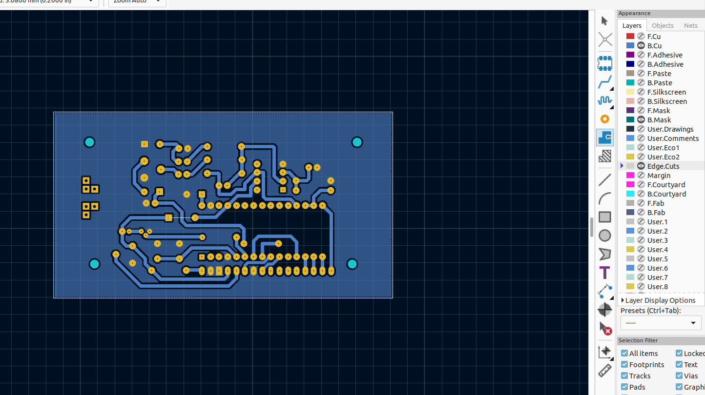
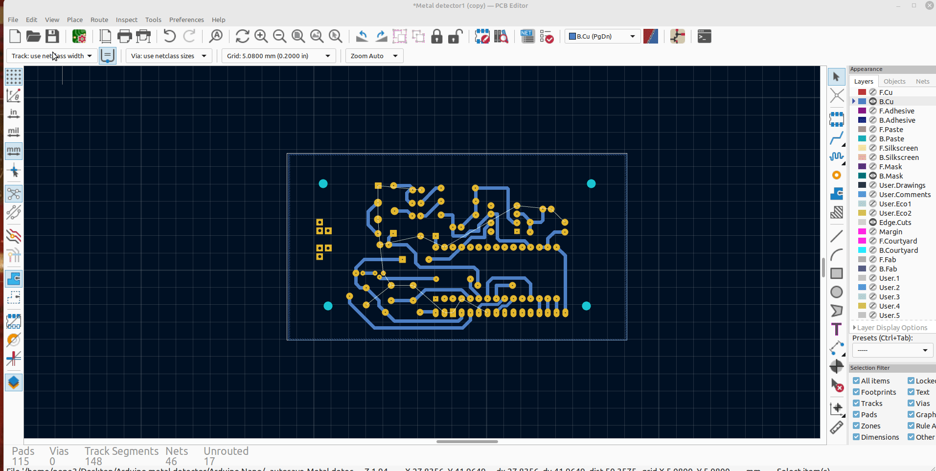
Here is the board I want to make a stencil out of:
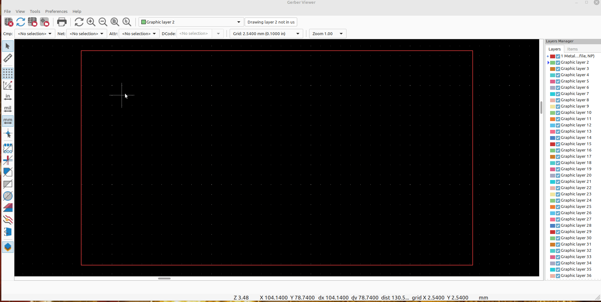
The first step is to output a gerber file so I can print out a pdf of the tracks and pads:
Then I can import the produced file into gerber viewer, which is part of Kicad to print it out to a pdf file:
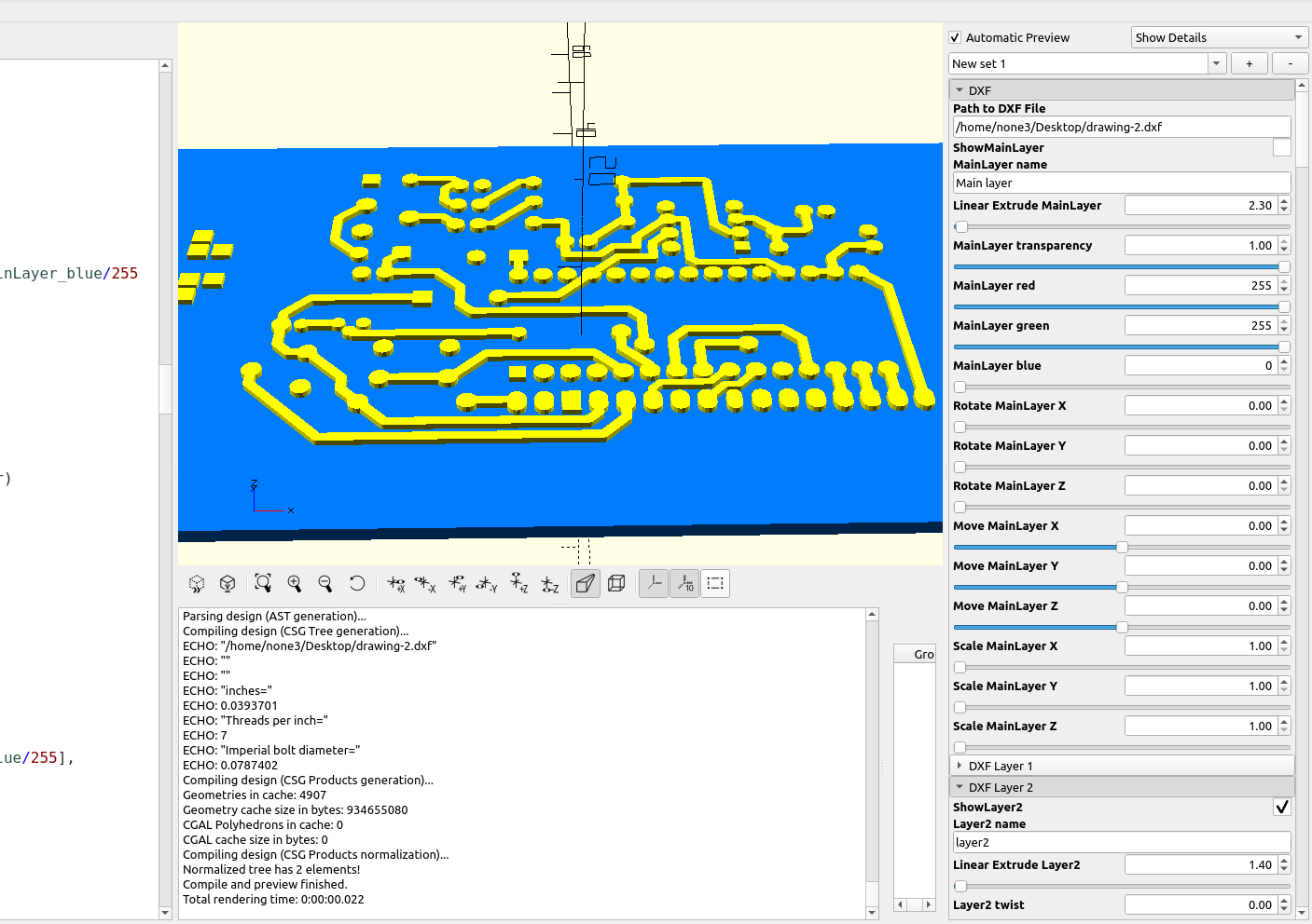
Then I can import the pdf into Inkscape, this part gets a little tricky because you have to click on the traces and then the background (white part) of the pdf several times in order to remove the back ground, once one of the the traces is selected (highlighted) you should be able to move the background and delete it:
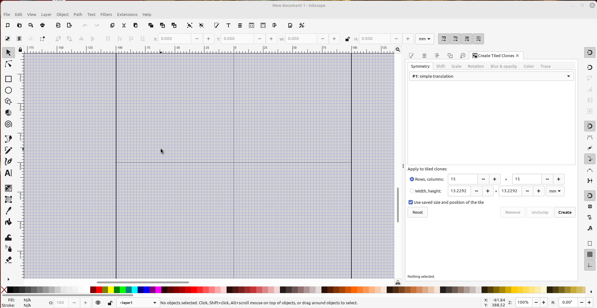
The next step is kind of tricky also, if you don't get all of the traces converted to paths they will not export properly and will be full of artifacts when you import them into openscad. The best method I have found is to select all of the pads and traces, convert objects to paths, strokes to paths, select same fill color, then union the paths. Then you can add extra nodes so the circular pads are round and convert them to lines:
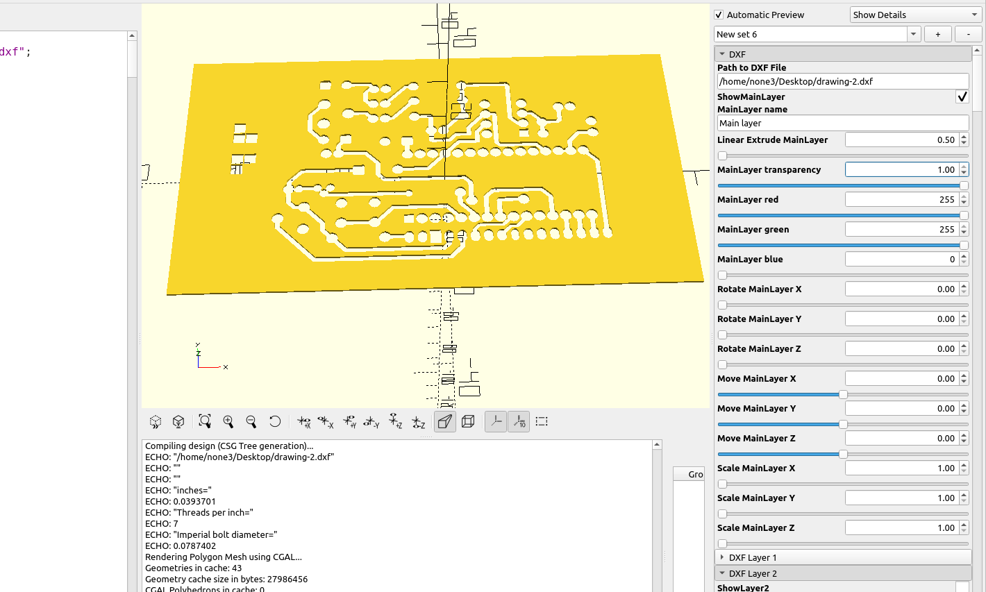
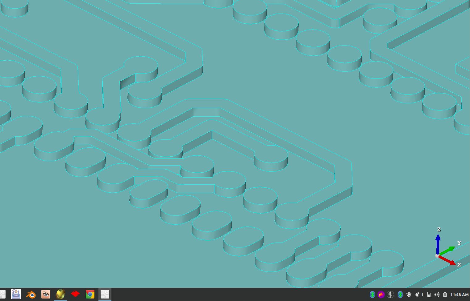
All of the traces and pads should look good when you import the Dxf into OpenScad, if not then they didn't get converted to paths properly:

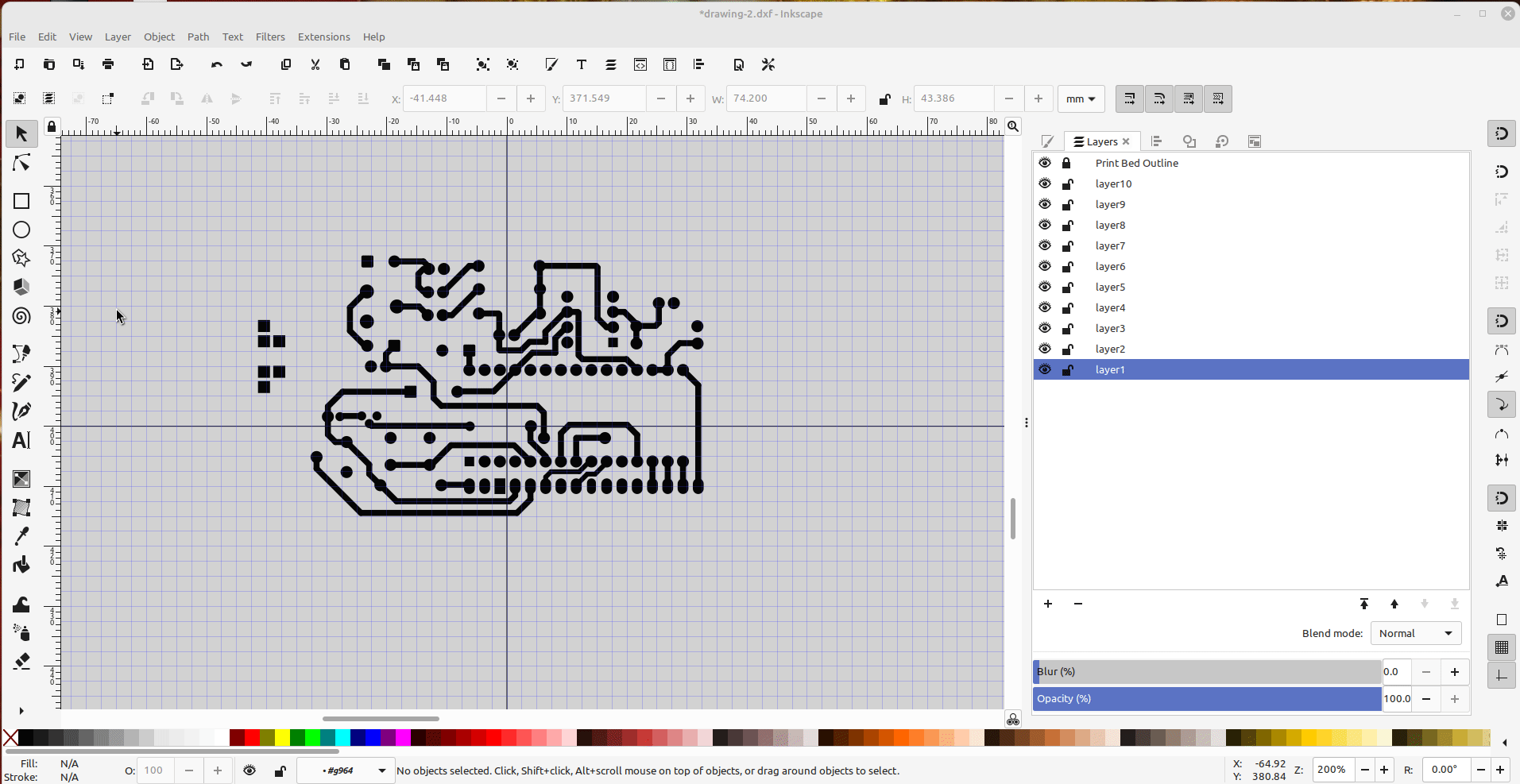
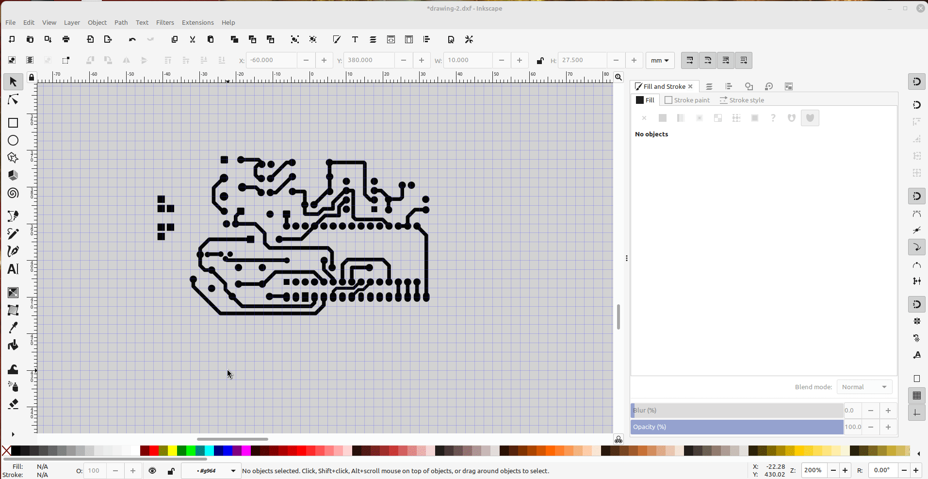
The last step is to make a frame around the stencil by making a rectangle on layer 2, I set the opacity so I could see the traces and pads to align it. Since the two layers overlap one another when the Dxf file is imported into the Inkscape2Openscad template "main layer", the pads and traces will be holes and the rectangle will be the stencil frame. Then all that is left is to extrude the the stencil to the desired height and print it out.
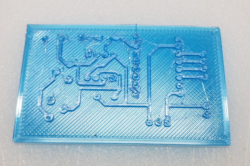
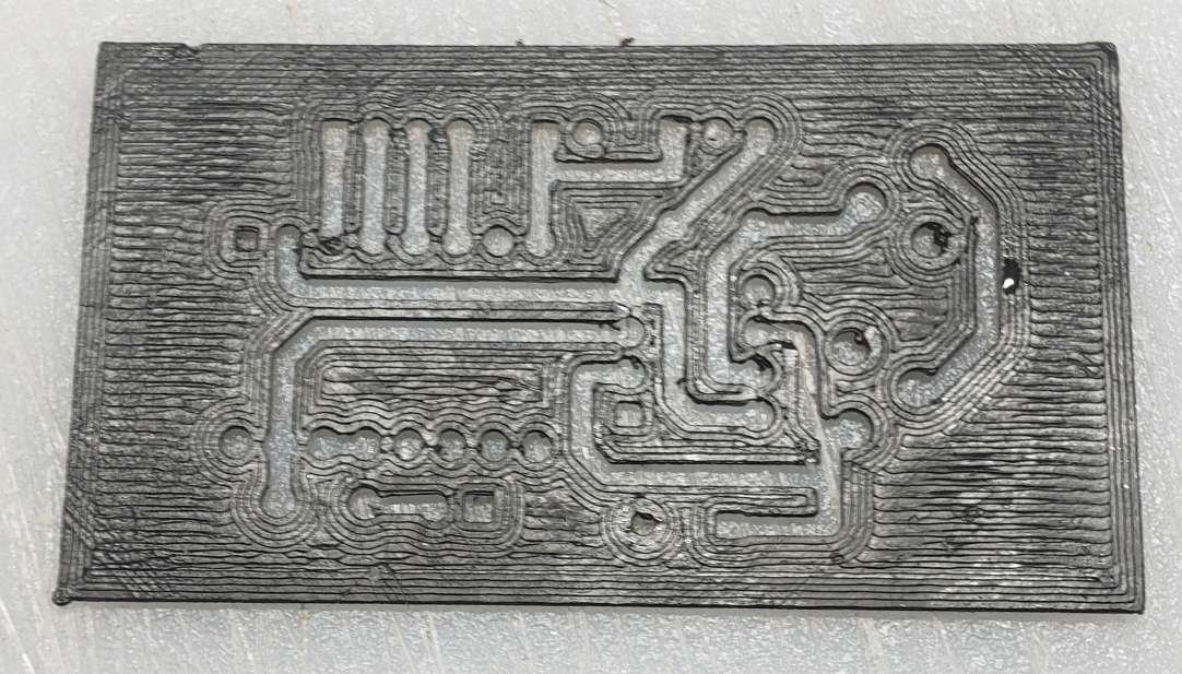
A finished print in PLA, 0.08 layer height, 0.08 first layer, 100% infill, 1mm thick stencil, 1hr 4min print time.
It turns out that ABS works great for making stencils, in part 2 I will be making a pcb for a filament spooler speed controller.
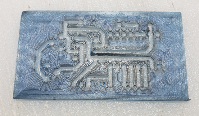
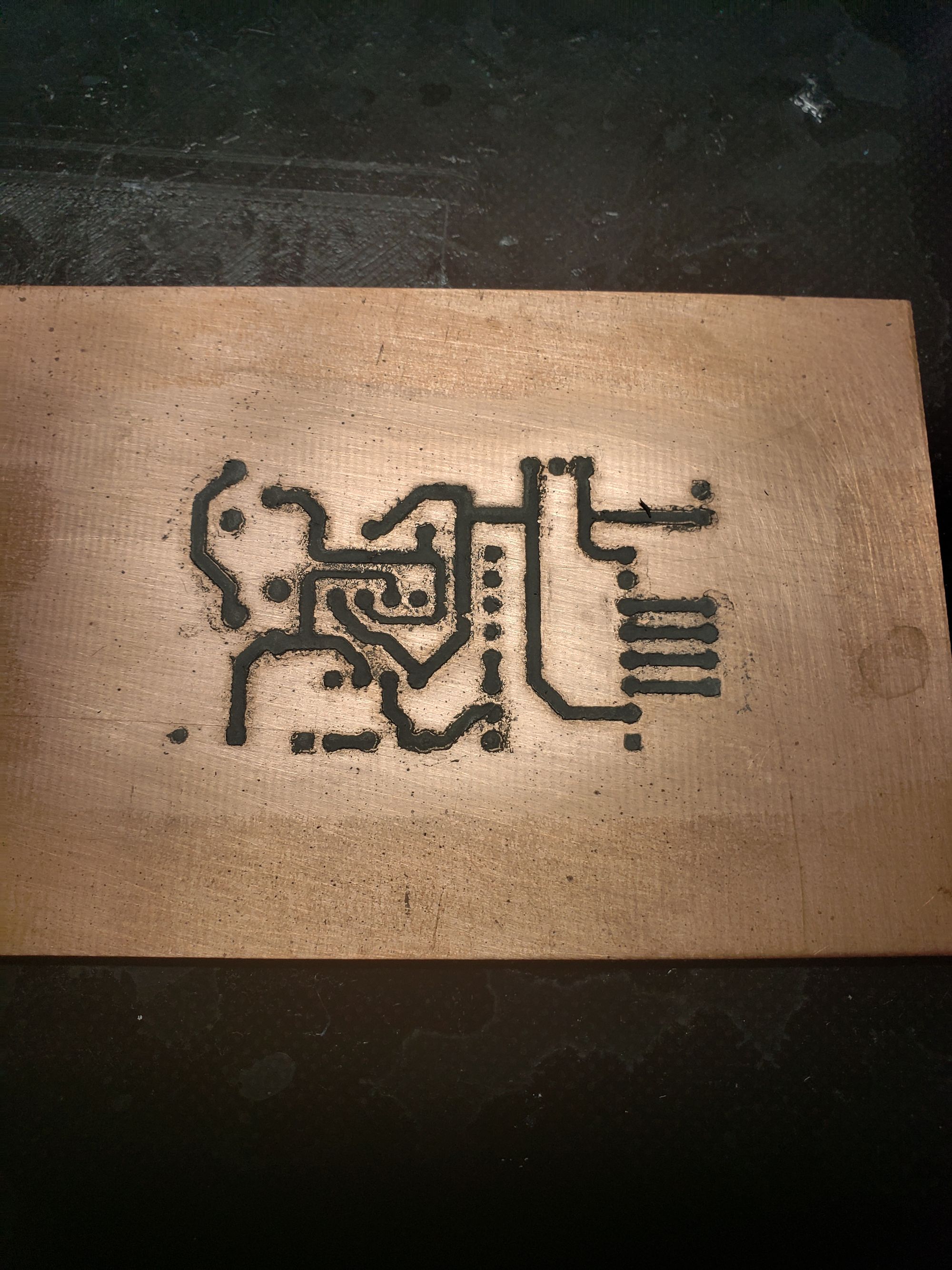
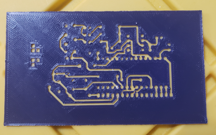
Do stencils work for making etch resist patterns for copper clad boards? Yes, here is a board I used spray paint on, you can see some over spray near the edges of the traces which will clean up with a small paint brush, this happened because I got in a hurry> by using some water soluble glue like modpodge on the stencil before putting it on the board it will stick down better and not allow the over spray under the stencil, you just have to let the paint dry before soaking it in water to remove the stencil.